使用寬帶電壓和電流反饋運算放大器時的應用基礎

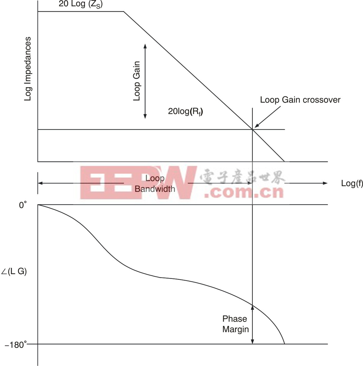
The CFB uses a unity-gain buffer across the two inputs. This forces the inverting node voltage to follow the non-inverting input voltage. That buffer is intended to present a low impedance to the inverting port, where a low level error current may be sensed and passed on to the output through a transimpedance gain. It is this internal transimpedance gain, Z(s), which acts in the same fashion as the VFB A(s) to provide a high DC gain with a dominant pole.
When the loop is closed, the same desired gain is achieved; but the loop-gain terms are very different. The CFB amplifier has a loop gain set by the forward transimpedance gain compared to the feedback impedance.Figure 4plots the loop gain and phase for a typical CFB amplifier, where the feedback element is assumed to introduce no phase shift in this simplified analysis.
(Click to Enlarge Image)
Figure 4. Current feedback (CFB) loop gain and phase plots. X-axis is log frequency.
This plot looks very similar to the VFB plot except that the external element setting the loop gain is the feedback impedance alone. The greatest difference between the VFB and CFB amplifier is that the loop gain can be set separately from the signal gain using the feedback impedance. The feedback impedance becomes an independent compensation element, where the gain can then be set using the normal gain equations from whatever impedance value is selected for RF. This approach gives what is sometimes calledgain bandwidth independencefor the CFB amplifier. (See Reference 1 for a more detailed discussion.)
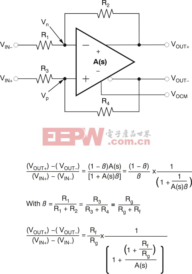
The final type of amplifier to be considered here is the new fully differential amplifier (FDA).Figure 5shows the configuration and closed loop transfer function for this type of amplifier.
(Click to Enlarge Image)
Figure 5. Fully differential amplifier (FDA) structure and transfer function.
If the two feedback networks are allowed to be unmatched, the transfer function is fairly complicated. If they have a matched divider ratio (see Figure 5), the equations simplify to be the same as the inverting VFB transfer function. The effect of the separate common-mode loop is not shown. This loop acts to servo the average output voltage to a value set by a VOCMinput pin voltage (seeReference 2for a more complete discussion of the FDA topology). For applications considered in this article, the FDA is treated as differential VFB device.
Application imperatives


評論