使用寬帶電壓和電流反饋運算放大器時的應用基礎

Here, the amplifier operates on a single +12 V supply and the filtered differential source is driven through blocking capacitors to the mid-supply referenced termination impedance. The differential gain is set to 6 V/V with a dc blocking capacitor in series with the gain resistor to further attenuate low-frequency noise and reduce output differential offset voltage.
Whether that capacitor is present in the circuit or not, the mid-supply reference on each non-inverting input shows up as the output common mode voltage as well. This circuit demonstrates a typical 1:2 step-up transformer at the output to a 100 Ω load, giving a nominal differential load of 50 ohms.
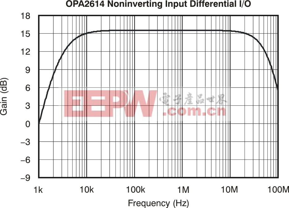
This circuit is often implemented using dual current feedback op amps (such as the OPA2677) but can give lower output noise using a decompensated dual voltage feedback op amp (for example, the OPA2614).Figure 12shows the simulated frequency response for this circuit showing about 50 MHz bandwidth—more than adequate for most DSL line driver applications.
(Click to Enlarge Image)
Figure 12. Non-inverting differential I/O small-signal frequency response.
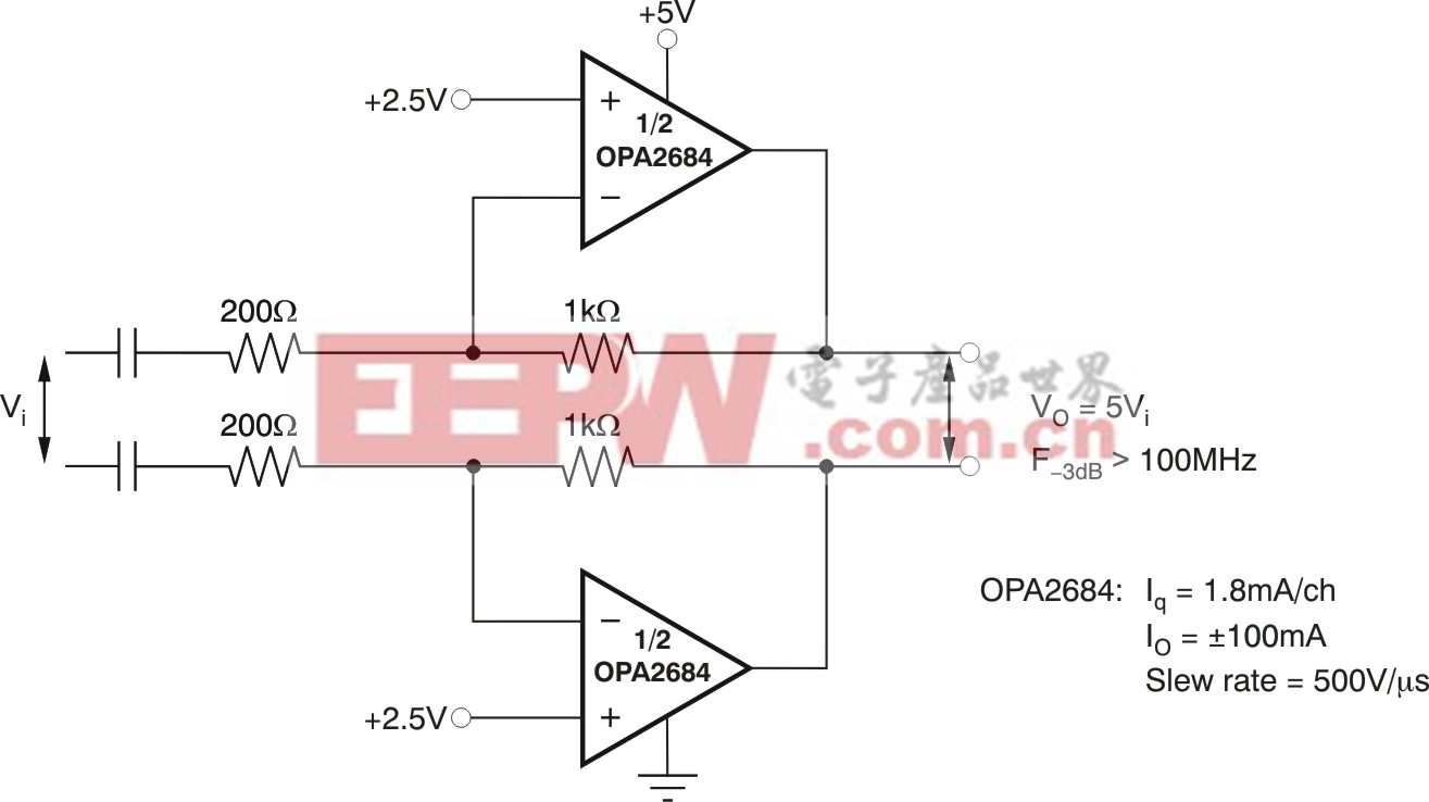
In the inverting input, differential I/O implementation, the differential input impedance is the sum of the two gain resistors; the output common-mode voltage depends on the dc voltage applied to the non-inverting inputs and the dc gain for that signal path, along with the dc common-mode voltage of the source. If the sources are capacitively or transformer-coupled, the common-mode voltage applied to the non-inverting inputs will have a gain of one to the output.
Figure 13shows an inverting differential I/O using the very low power OPA2684 dual CFB in a single +5 V supply with a mid-supply common-mode reference and an ac-coupled input interface.
(Click to Enlarge Image)
Figure 13. Low power, inverting differential I/O using the OPA2684.
This circuit provides a common-mode output of 2.5 V with a differential gain of five and >100 MHz bandwidth while using only 3.6 mA total quiescent supply current.
Figure 13 also shows a differential ac input impedance of 400 ohms. One adv


評論