薄膜晶體管和超大規模集成電路:競爭與合作

4. Summary
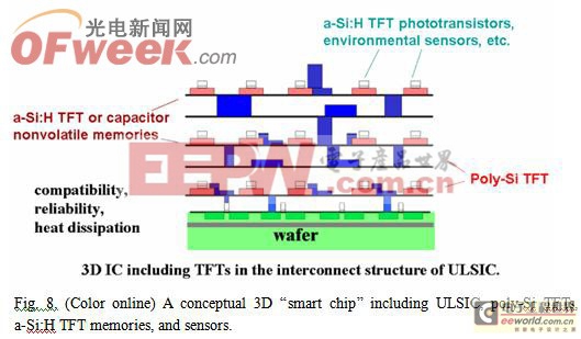
TFT and ULSIC are originated from the same concept. They both have been developed into gigantic industries with separate markets. Originally, TFT fabrication processes were derived from ULSIC processes. However, due to its unique temperature and substrate requirements, new knowledge on process chemistry and physics has been obtained, which is potentially important for the production of future nanodimension MOSFETs in large-size wafers. In this paper, the author compared and discussed the a-Si:H TFT, poly-Si TFT, and ULSIC technologies with respect to materials, processes, and devices. In the long term, their main applications will be in different fields due to different strengths and restrictions. However, in certain areas, these technologies may be integrated into one product such as the 3D ‘‘smart chip’’.
Acknowledgement
The author would like to acknowledge his graduate students and postdoctoral scholars for their dedicated work in both TFT and ULSIC areas. He also thanks financial supports from various funding agencies, such as NSF, other government agencies, and industry companies. The author also acknowledges the precious hands-on experience he gained from near two decades of industry service in
1) R. G. Arns:
2) Y. Kuo: ECS Trans. 6 (2007) No. 4, 121.
3) Y. Kuo: in Amorphous Silicon Thin Film Transistors, ed. Y. Kuo (Kluwer,
4) T. Tsukada: IEEE Trans. Electron Devices 38 (1991) 2689.
5) IRTS Factory Integration TWG, ‘‘
6) Economics Report, IC knowledge, Chap. 2 (http://www.icknowledge. com/our_products/Chapter PERCENT_202.pdf).
7) Y. Ishii: AM-FPD 06 Dig. Tech. Pap. 2006, p. 1.
8) Y. Kuo: in Amorphous Silicon Thin Film Transistors, ed. Y. Kuo (Kluwer,
9) C. D. Dimitrakopoulos and D. J. Mascaro: IBM J. Res. Dev. 45 (2001) 11.
10) P. F. Carcia, R. S. McLean, M. H. Reilly, and G. Nunes, Jr.: Appl. Phys. Lett. 82 (2003) 1117.
11) Y. Kuo: AM-FPD 06 Dig. Tech. Pap., 2006, p. 77.
12) T. Ikeda, Y. Shionoiri, T. Atsumi, A. Ishikawa, H. Miyake, Y. Kurokawa, K. Kato, J. Koyama, S. Yamazaki, K. Miyata, T. Matsuo, T. Nagai, Y. Hirayama, Y. Kubota, T. Muramatsu, and M. Katayama: SID Int. Symp. Dig. Tech. Pap. 35 (2004) 860.
13) Y. Yamomoto and A. T. Voutsas: ECS Trans. 3 (2006) No. 8, 11.
14) H. Hayama: ECS Trans. 3 (2006) No. 8, 3.
15) S. Uchikoga and
16) T. Takayama, Y. Ohno, Y. Goto, A. Machida, M. Fujita, J. Maruyama, K. Kato, J. Koyama, and S. Yamazaki: VLSI Technology Dig. Tech. Pap., 2004, p. 230.
17) J. Koyama, Y. Kurokawaa, T. Ikeda, M. Endo, H. Dembo, D. Kawae, T. Inoue, M. Kozuma, D. Ohgarane, S. Saito, K. Dairiki, H. Takahashi, and S. Yamazaki: ECS Trans. 8 (2007) No. 1, 57.
18) N. Saputra, M. Danesh, A. Baiano, R. Ishihara, J. R. Long, J. W. Metselaar, C. I. M. Beenakker, N. Karaki, Y. Hiroshima, and S. Inoue: Proc. European Solid-State Device Research Conf. (ESSDERC), 2007, C
19) S.-I. Hsieh, H.-T. Chen, Y.-C. Chen, C.-L. Chen, and Y.-C. King: IEEE Electron Device Lett. 27 (2006) 272.


評論