Quicklogic ArcticLink可編程連接平臺設計方案

ArcticLink可編程連接解決方案平臺采用0.18um六層金屬CMOS工藝制造,內核電壓為1.8V,I/O電壓可設定為1.8V,2.5V和3.3V. ArcticLink的邏輯單元為640個,集成了高速USB 2.0 OTG控制器, SD/SDIO/MMC/CE-ATA主控制器, ASSP/FPGA接口,以及靈活的可編程架構,可編程I/O,非常低功耗模式和安全鏈接.本文介紹了ArcticLink主要特性, 解決方案平臺方框圖, 連接解決方案方框圖,以及各種USBOTG連接框圖,在汽車內裝藍牙免提,智能手機,PND/PMP和ePOS的應用框圖.
The QuickLogic ArcticLink Solution Platform is fabricated on a 0.18 μm, six layer metal CMOS process. The core voltage is 1.8 V. The I/O voltage input tolerance and output drive can be set as 1.8 V, 2.5 V, and 3.3 V.
ArcticLink 器件亮點:
Hi-Speed USB 2.0 OTG Controller
Single port OTG with embedded high-speed PHY
Optional 12-signal ULPI interface
Full-speed CEA-936-A mini-USB analog carkit interface
Dedicated DMA controller
High-speed up to 480 Mbits/sec.
SD/SDIO/MMC/CE-ATA Host Controller
SD/SDIO 1-bit or 4-bit up to 52 MHz with Secure Digital High Capacity (SDHC) support
CE-ATA 1-bit, 4-bit or 8-bit up to 52 MHz
MMC 1-bit, 4-bit or 8-bit up to 52 MHz
High-speed and flexible to support multiple storage options and SDIO peripherals
ASSP/FPGA Interface
8 Kbytes scratchpad memory
Flexible Host interface for USB and SD/SDIO/MMC/CE-ATA ports
DMA and power management functions
Direct memory aperture for peripheral subsystems
Flexible Programmable Fabric
0.18 μm, six layer metal CMOS process
1.8 V core voltage, 1.8/2.5/3.3 V drive capable I/Os
36 Kbits of SRAM C seven dual-port 4-Kbit high performance SRAM blocks
Embedded synchronous/asynchronous FIFO controllers
One user configurable clock manager (CCM) (110-ball WLCSP and 196-ball TFBGA packages only)
Up to 120 programmable I/Os available
100,000 system gates
Nonvolatile, instant-on
IEEE 1149.1 boundary scan testing compliant
Programmable I/O
Bank programmable drive strength
Bank programmable slew rate control
Independent I/O banks capable of supporting multiple I/O standards in one device
Native support for DDRIOs (196-ball package only)
Bank programmable I/O standards: LVTTL, LVCMOS, and LVCMOS18
Can be used for level shifter and I/O voltage translator
Very Low Power (VLP) Mode
The QuickLogic ArcticLink Solution Platform has a special VLP pin which can enable a low power sleep mode that significantly reduces the overall power consumption of the device by placing the device in standby.
Enter/exit VLP mode from/to normal operation in less than 250 μs (typical)
Security Links
There are several security links to disable JTAG access to the device. Programming these optional links completely disables access to the device from the outside world and provides an extra level of design security not possible in SRAM-based FPGAs.
JTAG
QuickLogic ArcticLink Solution Platform supports IEEE 1149.1 boundary scan or post-manufacturing testability. External access to this feature can be completely disabled.
ArcticLink QL1A100主要特性列表: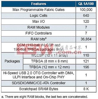
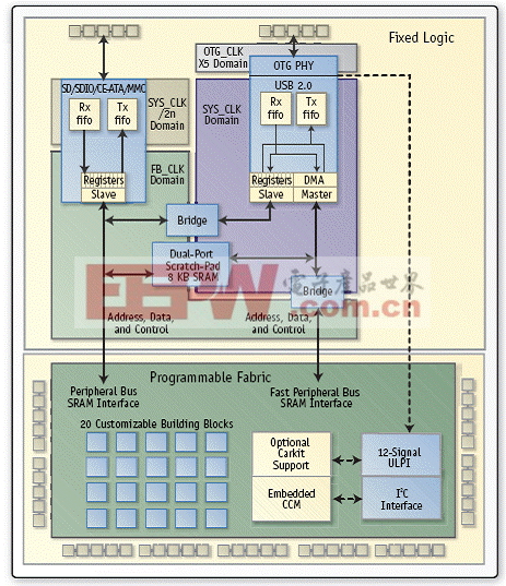
圖1.ArcticLink 解決方案平臺方框圖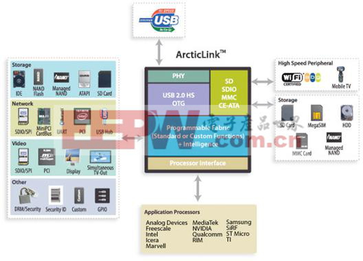
圖2.ArcticLink 連接解決方案方框圖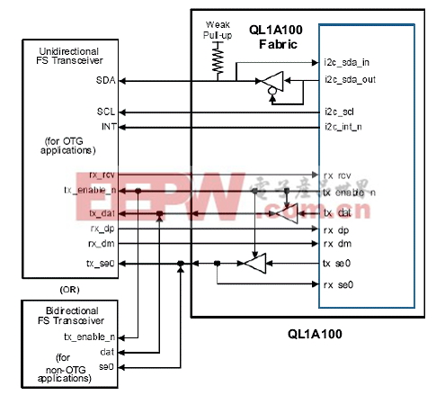


評論