基于LPC2939設計的MCU USB接口技術

LPC2939集成了兩個TCM 的ARM968E-S CPU 核的MCU,工作頻率高達125MHz,并集成了全速USB 2.0主/OTG/設備控制器,CAN和LIN,56kB SRAM,768kB閃存以及外接存儲器接口,三個10位ADC,多個串行和并行接口.主要用在消費類電子,工業,醫療和通信市場.本文介紹了LPC2939主要特性, 方框圖,以及各種USB,USB OTG接口方框圖.
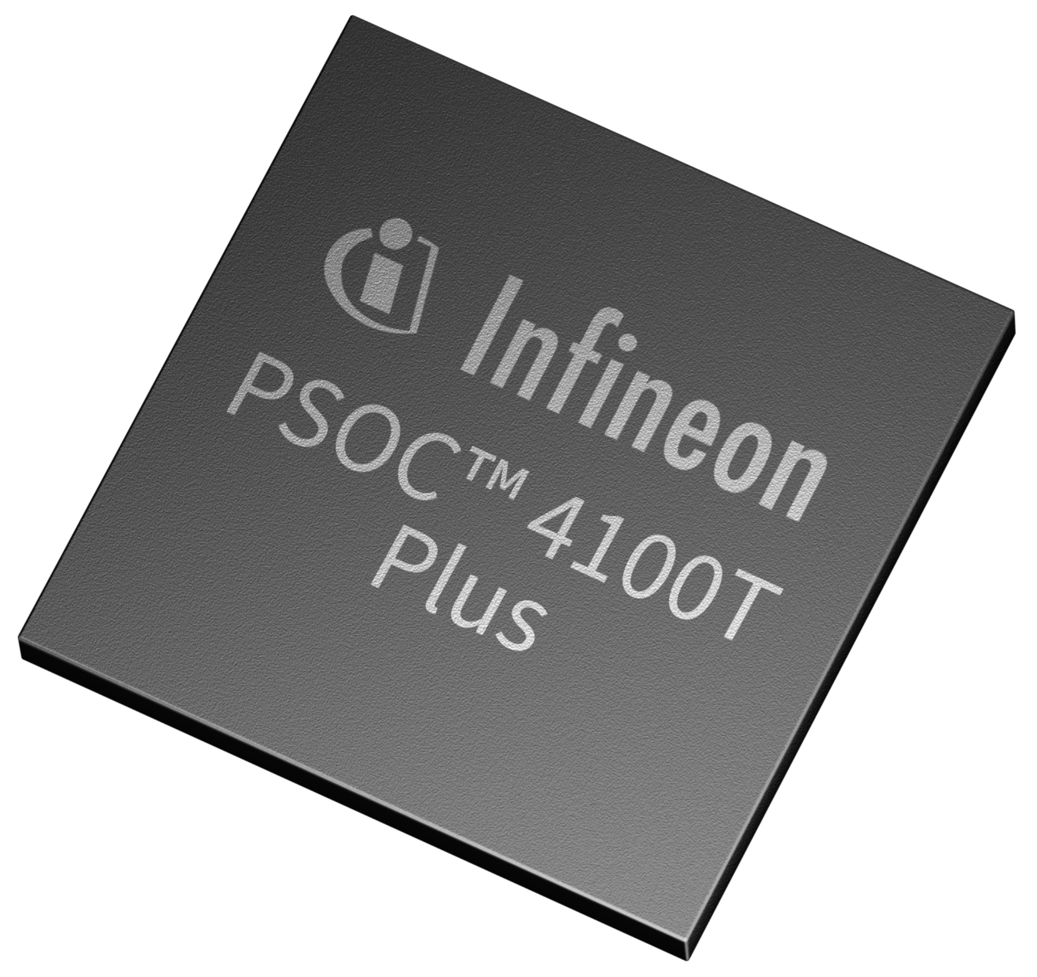
LPC2939: ARM9 microcontroller with CAN, LIN, and USB
The LPC2939 combine an ARM968E-S CPU core with two integrated TCM blocks operating at frequencies of up to 125 MHz, Full-speed USB 2.0 Host/OTG/Device controller, CAN and LIN, 56 kB SRAM, 768 kB flash memory, external memory interface,three 10-bit ADCs, and multiple serial and parallel interfaces in a single chip targeted at consumer, industrial, medical, and communication markets. To optimize system power
consumption, the LPC2939 has a very flexible Clock Generation Unit (CGU) that provides dynamic clock gating and scaling.
LPC2939主要特性和優勢:
ARM968E-S processor running at frequencies of up to 125 MHz maximum.
Multilayer AHB system bus at 125 MHz with four separate layers.
On-chip memory:
Two Tightly Coupled Memories (TCM), 32 kB Instruction (ITCM), 32 kB Data TCM (DTCM)
Two separate internal Static RAM (SRAM) instances; 32 kB SRAM and 16 kB SRAM
8 kB ETB SRAM, also usable for code execution and data
768 kB high-speed flash program memory
16 kB true EEPROM, byte-erasable/programmable
Dual-master, eight-channel GPDMA controller on the AHB multilayer matrix which can be used with the SPI interfaces and the UARTs, as well as for memory-to-memory transfers including the TCM memories
External Static Memory Controller (SMC) with eight memory banks; up to 32-bit data bus; up to 24-bit address bus
Serial interfaces:
USB 2.0 full-speed Host/OTG/Device controller with dedicated DMA controller and on-chip device PHY
Two-channel CAN controller supporting FullCAN and extensive message filtering
Two LIN master controllers with full hardware support for LIN communication. The LIN interface can be configured as UART to provide two additional UART interfaces.
Two 550 UARTs with 16-byte Tx and Rx FIFO depths, DMA support, modem control, and RS-485/EIA-485 (9-bit) support
Three full-duplex Q-SPIs with four slave-select lines; 16 bits wide; 8 locations deep;Tx FIFO and Rx FIFO
Two I2C-bus interfaces
Other peripherals:
One 10-bit ADC with 5.0 V measurement range and eight input channels with conversion times as low as 2.44 s per channel
Two 10-bit ADCs, 8-channels each, with 3.3 V measurement range provide an additional 16 analog inputs with conversion times as low as 2.44 s per channel. Each channel provides a compare function to minimize interrupts.
Multiple trigger-start option for all ADCs: timer, PWM, other ADC, and external signal input
Four 32-bit timers each containing four capture-and-compare registers linked to I/Os
Four six-channel PWMs (Pulse-Width Modulators) with capture and trap functionality
Two dedicated 32-bit timers to schedule and synchronize PWM and ADC
Quadrature encoder interface that can monitor one external quadrature encoder
32-bit watchdog with timer change protection, running on safe clock
Up to 152 general-purpose I/O pins with programmable pull-up, pull-down, or bus keeper
Vectored Interrupt Controller (VIC) with 16 priority levels
Up to 22 level-sensitive external interrupt pins, including USB, CAN and LIN wake-up features
Configurable clock-out pin for driving external system clocks
Processor wake-up from power-down via external interrupt pins and CAN or LIN activity
Flexible Reset Generator Unit (RGU) able to control resets of individual modules
Flexible Clock-Generation Unit (CGU) able to control clock frequency of individual modules:
On-chip very low-power ring oscillator; fixed frequency of 0.4 MHz; always on to provide a Safe_Clock source for system monitoring
On-chip crystal oscillator with a recommended operating range from 10 MHz to 25 MHz. PLL input range 10 MHz to 25 MHz.
On-chip PLL allows CPU operation up to a maximum CPU rate of 125 MHz
Generation of up to 11 base clocks
Seven fractional dividers
Second, dedicated CGU with its own PLL generates USB clocks and a configurable clock output
Highly configurable system Power Management Unit (PMU):
clock control of individual modules
allows minimization of system operating power consumption in any configuration
Standard ARM test and debug interface with real-time in-circuit emulator
Boundary-scan test supported
ETM/ETB debug functions with 8 kB of dedicated SRAM also accessible for application code and data storage
Dual power supply:
CPU operating voltage: 1.8 V 5 %
I/O operating voltage: 2.7 V to 3.6 V; inputs tolerant up to 5.5 V
208-pin LQFP package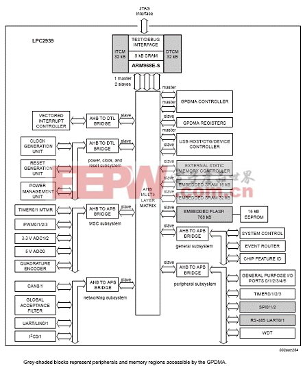
圖1.LPC2939方框圖
圖2.LPC2939自供電設備USB接口方框圖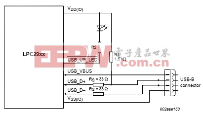


評論