基于LatticeXP2設計的FPGA標準評估技術

LatticeXP2器件包括基于查找表(LUT)的 FPGA以及非易失閃存單元(flexiFLASH)。LatticeXP2系列器件的LUT從5K到40K,分布是RAM從10K到83Kb,EBR SRAM從166Kb到885Kb,EBR SRAM區塊從9到48個,sysDSP從3個到8個,18x18乘法器從12個到32個,可用的I/O從172個到540個,GPLL從2個到4個。工作電壓1.2V,主要用在對成本敏感的市場如消費類電子,汽車電子,醫療和工業,網絡和計算。
LatticeXP2主要特性: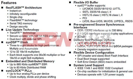
LatticeXP2系列產品: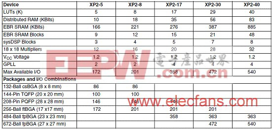
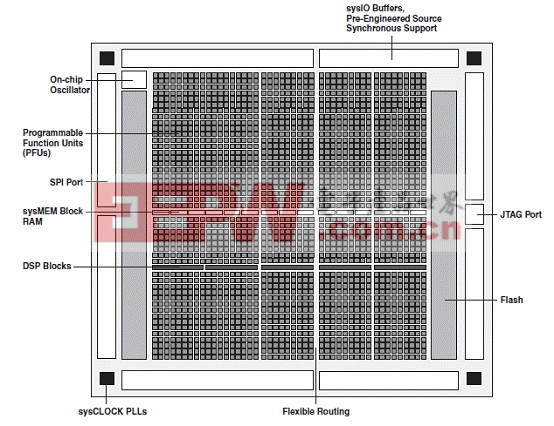
圖1。LatticeXP2-17器件簡化方框圖(頂視圖)
LatticeXP2 devices are ideal for a variety of applications in cost sensitive markets such as Consumer, Automotive, Medical Industrial, Networking and Computing
LatticeXP2標準評估板
LatticeXP2 Standard Evaluation Board
The LatticeXP2™ Standard Evaluation Board provides a convenient platform to evaluate, test and debug user designs. The board features a LatticeXP2-17 FPGA in a 484 fpBGA package. The LatticeXP2 I/Os are connected to a rich variety of interfaces described later in this document.
This document (including the schematics in the appendix) describes LatticeXP2 Standard Evaluation Boards marked as Rev 000. This marking can be seen on the etching on the back of the printed circuit board, under the Lattice Semiconductor logo.
The LatticeXP2 is a third-generation non-volatile FPGA device. It combines a Look-up Table (LUT) based FPGA fabric with Flash Non-volatile cells in a flexiFLASH™ architecture. The flexiFLASH approach provides benefits such as instant-on, small footprint, on chip storage with FlashBAK™ embedded block memories and Serial TAG memory and design security. The LatticeXP2 also supports live updates with TransFR™, 128-bit AES Encryption and Dual-Boot technologies. The LatticeXP2 devices include LUT-based logic, distributed and embedded memory, Phase Locked Loops (PLLs), pre-engineered source synchronous I/O and enhanced sysDSP™ blocks.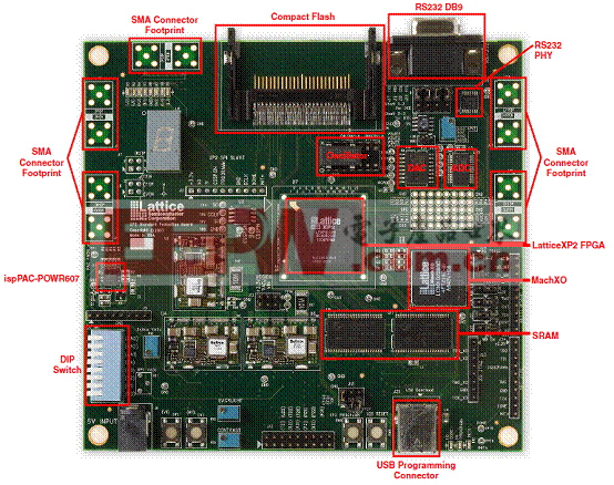
圖2。LatticeXP2標準評估板外形圖
LatticeXP2標準評估板主要特性:
LatticeXP2 Standard Evaluation Board featuring
LatticeXP2-17 FPGA in 484fpBGA package (LFXP2-17E-6F484C)
On-board Asynch SRAM memory (256Kx32 providing 1Mbyte)
A/D converter (Burr Brown ADS7842)
D/A converter (Burr Brown DAC7617)
10K digital POT
RS232 DB9 female connector
Compact Flash connector
8-bit switch
8 general purpose LEDs
4 push-button switches
7-segment LED
Built-in USB download capability (includes MachXO device)
Selectable I/O voltage
SMA connectors for clock and general purpose I/O
PAC607 power manager
on-board oscillator (dip socket)
Proto/test area
SPI flash memory for alternate configuration
Power via Bellnix DC power control modules
LCD connector 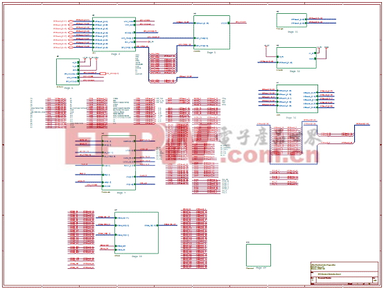
圖3。LatticeXP2標準評估板電路圖(1)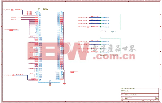
圖4。LatticeXP2標準評估板電路圖(2):電源和配置


評論