ADIADM106610個(gè)電源監(jiān)視和時(shí)序控制解決方案

The ADM1066 Super Sequencer? is a configurable supervisory/ sequencing device that offers a single-chip solution for supply monitoring and sequencing in multiple-supply systems. In addition to these functions, the ADM1066 integrates a 12-bit ADC and six 8-bit voltage output DACs. These circuits can be used to implement a closed-loop margining system that enables supply adjustment by altering either the feedback node or reference of a dc-to-dc converter using the DAC outputs.
Supply margining can be performed with a minimum of external components. The margining loop can be used for in-circuit testing of a board during production (for example, to verify board func-tionality at ?5% of nominal supplies), or it can be used dynamically to accurately control the output voltage of a dc-to-dc converter。
ADM1066主要特性:
Complete supervisory and sequencing solution for up to 10 supplies
10 supply fault detectors enable supervision of supplies to
0.5% accuracy at all voltages at 25°C
1.0% accuracy across all voltages and temperatures
5 selectable input attenuators allow supervision of supplies to 14.4 V on VH
6 V on VP1 to VP4 (VPx)
5 dual-function inputs, VX1 to VX5 (VXx)
High impedance input to supply fault detector with thresholds between 0.573 V and 1.375 V
General-purpose logic input
10 programmable driver outputs, PDO1 to PDO10 (PDOx)
Open-collector with external pull-up
Push/pull output, driven to VDDCAP or VPx
Open collector with weak pull-up to VDDCAP or VPx
Internally charge-pumped high drive for use with external N-FET (PDO1 to PDO6 only)
Sequencing engine (SE) implements state machine control of PDO outputs
State changes conditional on input events
Enables complex control of boards
Power-up and power-down sequence control
Fault event handling
Interrupt generation on warnings
Watchdog function can be integrated in SE
Program software control of sequencing through SMBus
Complete voltage-margining solution for 6 voltage rails
6 voltage output 8-bit DACs (0.300 V to 1.551 V) allow voltage adjustment via dc-to-dc converter trim/feedback node
12-bit ADC for readback of all supervised voltages
2 auxiliary (single-ended) ADC inputs
Reference input (REFIN) has 2 input options
Driven directly from 2.048 V (±0.25%) REFOUT pin
More accurate external reference for improved ADC performance
Device powered by the highest of VPx, VH for improved redundancy
User EEPROM: 256 bytes
Industry-standard 2-wire bus interface (SMBus)
Guaranteed PDO low with VH, VPx = 1.2 V
Available in 40-lead, 6 mm × 6 mm LFCSP and 48-lead, 7 mm × 7 mm TQFP packages
ADM1066應(yīng)用:
Central office systems
Servers/routers
Multivoltage system line cards
DSP/FPGA supply sequencing
In-circuit testing of margined supplies
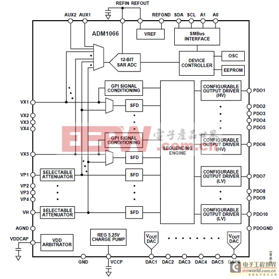
圖1. ADM1066方框圖

圖2. ADM1066應(yīng)用框圖
ADM106x評(píng)估板
Evaluation Kit for the ADM1062- ADM1069 Super Sequencers?
The ADM106x Evaluation Board is designed to provide all of the necessary stimuli to the ADM106x, showing the many features of the device in a compact, self contained environment. The following pages contain a simple block diagram of the functions on the board, followed by a detailed schematic of the board and finally, the tracking, power and silkscreen layers for board.
The two main features of the board are the programmable voltage circuits and the output indicator LED’s. There are eight programmable voltage circuits provided. The circuits are labeled VX1, VX2, VX3, VX4, VP1, VP2, VP3, VP4. These are programmable, via the Eval Board software, over a voltage range of 0.6V to 6V. Programming of these supplies is detailed in the software section of this Eval Note. The eight circuits provide voltages to eight of the ten inputs to the ADM106x. The inputs which do not have a programmable supply are VX5 (where a test point is available for the user for their own external input) and VH, which has 12V driving it directly (or alternatively, uses the programmable supply of VP4, if required).
The ten output indicator LED’s are labeled PDO1 to PDO10. These indicate a logic high on the output pins of the ADM106x. The LED’s for PDO1- 6 are dual colour LED’s. This is to indicate when a PDO is being used as a logic output or as a FET driver output. Green indicates a logic output while red indicates a FET driver output.
ADM106x評(píng)估板包括:
? Main Evaluation Board: This board contains all of the circuitry necessary to active stimulate the ADM1062-69 devices and monitor its response, such as programmable supplies, ADCs, LEDs, etc.
? Daughter-card Socket: A relevant daughter-card with a device socket is also supplied. There are three different daughter-card options for the main evaluation board depending on the package option- LFCSP, TQFP or LQFP. The daughter-card plugs directly into the main evaluation board and allows all the devices in their specific layouts to be used in conjunction with the main evaluation board. The correct one will be supplied for the devices included in the kit.
? Device Samples: Some loose samples of the device to be evaluated are included in a samples box. A single device should be placed in the socket before powering up the evaluation board.
? SMBus Cable: This cable connects the main evaluation board to a standard PC parallel connector. Power must be applied to the board separately if using this cable.
? USB Cable: This cable connects the main evaluation board to a standard PC USB port. Power for the evaluation board will also be provided by the PC USB interface.
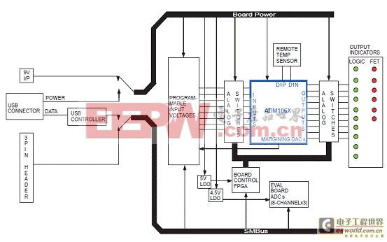
圖3.ADM106x評(píng)估板方框圖
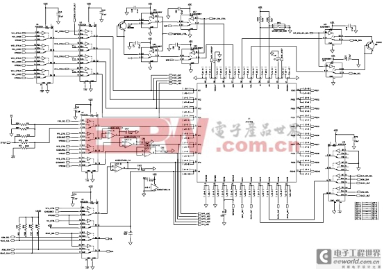
圖4.ADM106x評(píng)估板電路圖:ADM106x電路
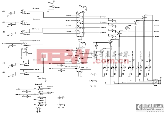
圖5.ADM106x評(píng)估板電路圖:ADM106x PDO輸出電路
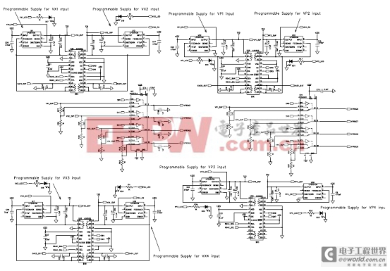
圖6.ADM106x評(píng)估板電路圖:可編程輸入電壓電路
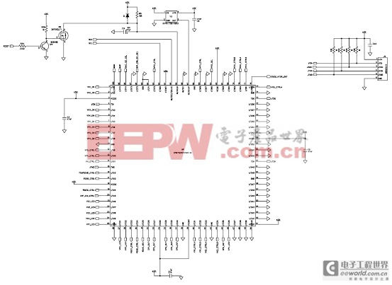
圖7.ADM106x評(píng)估板電路圖:板控制FPGA電路
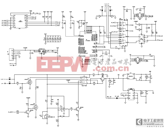
圖8.ADM106x評(píng)估板電路圖:板電源和USB接口電路

圖9.ADM106x評(píng)估板電路圖:板電壓測(cè)量電路
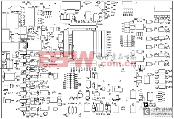
圖10.ADM106x評(píng)估板元件布局圖
詳情請(qǐng)見(jiàn):
http://www.analog.com/static/imported-files/data_sheets/ADM1066.pdf
和
http://www.analog.com/static/imported-files/eval_boards/adm106x_eb_pB.pdf


評(píng)論