ADIADP1853輸出20ADC-DC轉換解決方案

The ADP1853 is a wide range input, dc-to-dc, synchronous buck controller capable of running from commonly used 3.3 V to 12 V (up to 20 V) voltage inputs. The device nominally operates in current mode with valley current sensing providing the fastest step response for digital loads. It can also be configured as a voltage mode controller with low noise and crosstalk for sensitive loads.
The ADP1853 can be used as a master synchronization clock for the power system and for convenient synchronization between controllers. The CLKOUT signal can synchronize other devices in the ADP185x family such that slave devices are phase-shifted from the master to reduce the input ripple current, improve EMI, and reduce the size of the input bulk capacitance. The ADP1853 can also be configured as a slave device for current sharing. Additionally, the ADP1853 includes accurate tracking, precision enable, and power good functions for sequencing. The ADP1853 provides a high speed, high peak current gate driving capability to enable energy efficient power conversion. The device can be configured to operate in power saving mode by skipping pulses, reducing switching losses and improving efficiency at light load and standby conditions.
The accurate current limit allows design within a narrower range of tolerances and can reduce overall converter size and cost. The ADP1853 can regulate down to 0.6 V output using a high accuracy reference with ±1% tolerance over the temperature range from ?0℃ to 125℃.
With a wide range input voltage, the ADP1853 is designed to provide the designer with maximum flexibility for use in a variety of system configurations; loop compensation, soft start, frequency setting, power saving mode, current limit, and current sense gain can all be programmed using external components. In addition, the external RAMP resistor allows choosing optimal slope and VIN feedforward in both current and voltage mode for excellent line rejection. The linear regulator and the boot strap diode for the high-side driver are internal.
Protection features include undervoltage lock out, overvoltage, overcurrent/short circuit, and overtemperature.
ADP1853主要特性:
Input voltage range: 2.75 V to 20 V
Output voltage range: 0.6 V to 90% VIN
Maximum output current of more than 25 A
Current mode architecture with current sense input
Configurable to voltage mode
±1% output voltage accuracy over temperature
Voltage tracking input
Programmable frequency: 200 kHz to 1.5 MHz
Synchronization input
Internal clock output
Power saving mode at light load
Precision enable input
Power good with internal pull-up resistor
Adjustable soft start
Programmable current sense gain
Integrated bootstrap diode
Starts into a precharged load
Externally adjustable slope compensation
Suitable for any output capacitor
Overvoltage and overcurrent-limit protection
Thermal overload protection
Input undervoltage lockout (UVLO)
Available in 20-lead, 4 mm × 4 mm LFCSP
Supported by ADIsimPower?design tool
ADP1853應用:
Intermediate bus and POL systems requiring sequencing and tracking, including
Telecom base station and networking
Industrial and Instrumentation
Medical and healthcare
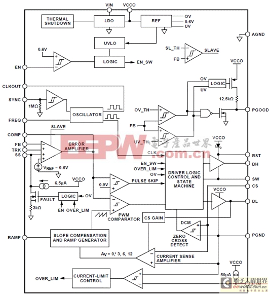
圖1.ADP1853方框圖
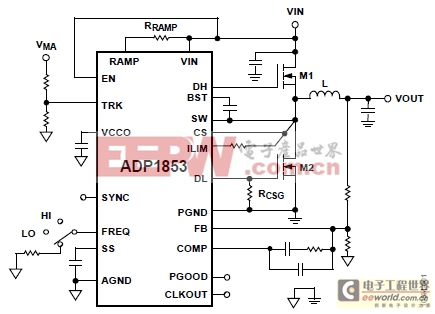
圖2.ADP1853典型應用電路圖
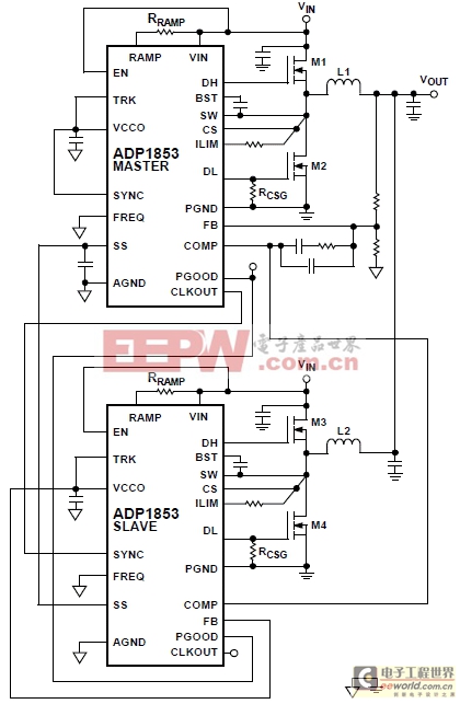
圖3.ADP1853兩相應用電路圖
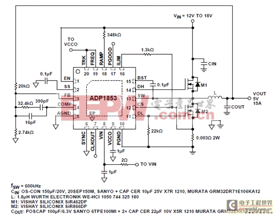
圖4.ADP1853 15A電流模式應用電路圖
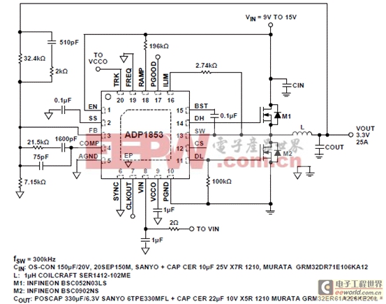
圖5.ADP1853 25A電壓模式應用電路圖
ADP1853降壓DC/DC控制器評估板
This document describes the design, operation, and test results of the ADP1853-EVALZ. The input voltage range for this evaluation board is 9 V to 15 V, and the regulated output voltage VOUT is set to 3.3 V with the maximum output current up to 20 A. The switching frequency (fSW) of 300 kHz is set to achieve high efficiency.
ADP1853評估板主要特性:
Input voltage range: 9 V to 15 V
Output voltage: 3.3 V
Output current: up to 20 A
Switching frequency: 300 kHz
Operates in PWM or PSM
Designed for evaluation of the ADP1853 functionality
Flexible and easy to re-configure and modify
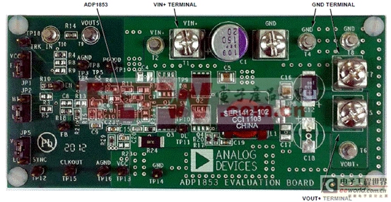
圖6.ADP1853評估板外形圖
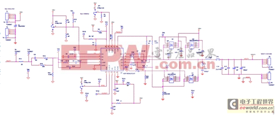
圖7.ADP1853評估板電路圖
ADP1853評估板材料清單:
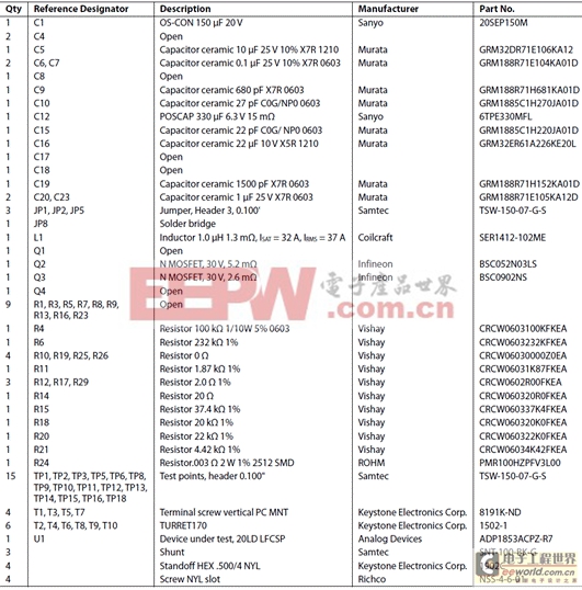
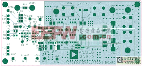
圖8.ADP1853評估板元件布局圖(頂層)
詳情請見:
http://www.analog.com/static/imported-files/data_sheets/ADP1853.pdf
和
http://www.analog.com/static/imported-files/user_guides/UG-431.pdf


評論