Simple Methods Reduce Input Ri

Abstract: Charge pumps are a form of DC-DC converter that rely on capacitors instead of inductors for energy storage and transfer. The absence of inductors makes them attractive in situations requiring a low-power auxiliary supply (output currents up to about 150mA). They use less circuit-board area, offer minimal component height, and are easy to use.
Charge pumps can have regulated or unregulated outputs. An unregulated charge pump either doubles or inverts the voltage that powers it and the output voltage is a function of the supply voltage. A regulated charge pump either boosts or inverts the supply voltage. Its output voltage is independent of the supply.
Techniques that reduce capacitor size and optimize output current—fast switching speed and low-on-resistance switches—also produce noise and transient ripple at the input supply pin. Noise can propagate back along the input supply pins, creating problems for crystal-controlled oscillators, VCOs, and other sensitive circuits with poor power-supply rejection. This article focuses on methods for reducing the noise.
Simplified Operation
First, consider a charge pump connected as an inverter. In the simplified version (Figure 1), operation is controlled by 2-phase clock signals with 50% duty cycles. The pump capacitor (charge-transfer component) is charged to VIN via closure of SW1A and SW1B. SW2A and SW2B are open at this time. On the next clock cycle, the closure of SW2A and SW2B connects the pump capacitor to COUT, thereby producing -VIN at the output.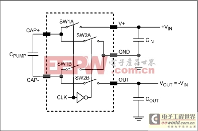
Figure 1. Simplified diagram of a charge pump connected as an inverter.
Next, connect the charge pump as a doubler (Figure 2). As before, operation is controlled by 2-phase, 50%-duty-cycle clock signals. The pump capacitor is the charge transfer device and is charged up to VIN by closure of SW2A and SW2B (SW1A and SW2B are open at this time). On the next clock cycle, the closure of SW1A and SW1B produces +2VIN at the output by connecting the pump capacitor to COUT.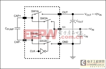
Figure 2. Simplified diagram of a charge pump connected as a doubler.
Input and output ripple is caused by rapid charging and discharging of the pump capacitor. An inverter circuit (Figure 3) built around the MAX665 charge pump and producing 5V across 51Ω, illustrates the input-ripple artifacts (Figure 4). (Ripple produced by the high-current, low-frequency (≤ 100kHz) MAX665 is easily measured.)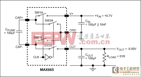
Figure 3. This charge-pump inverter circuit is used for measurements.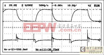
Figure 4. Input voltage and current ripple for standard inverter circuit: CIN = CPUMP = COUT = 100μF, RLOAD = 51Ω, VIN = +5.73V, and VOUT = -5.06V. Input current ripple (upper trace): 100mA/div. Input voltage ripple (lower trace): 200mV/div, AC coupled.
Ripple-reduction Methods
To reduce ripple, you must isolate ripple sources from the rest of the circuit. For best conversion efficiency in the charge pump, you should also minimize ESR and ensure that the input-, output-, and pump-capacitor values are as close as possible to those recommended in the data sheet. The following discussion covers four techniques for minimizing ripple and its effects.
1. Reducing ESR in the input capacitor implies multiple capacitors connected in parallel: N identical capacitors in parallel reduces the input ripple by N-1. Unfortunately, that approach is not very effective in terms of cost and pc-board area.
2. Instead, add an LC filter at the input supply pin (Figure 5). The additional filtering prevents ripple from propagating to other circuits via the input supply trace. As a second-order filter, the LC network minimizes the component count. In addition, its small series inductance produces a minimal voltage drop between the input supply and the charge pump.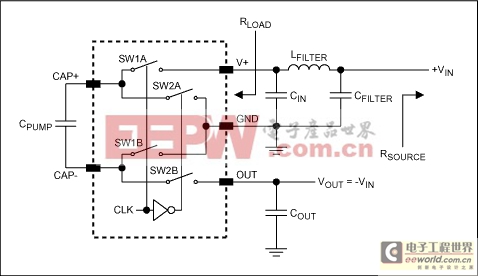
Figure 5. Charge-pump inverter with input LC filter.
The ripple-frequency fundamental equals the pump frequency (FCLOCK/2). Second-order filters attenuate at 40dB/decade, so the ideal filter frequency should be a minimum of one decade below the chosen FCLOCK/2.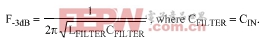
The inductor must handle dc currents greater than 1.5IOUT without saturation. For critical damping (ie., with no peaking),
The filter should be critically damped or close to it, given the low impedance values of RSOURCE and RLOAD. Critical damping is not essential to the circuit operation, however. Filtering remains effective even with some peaking at the point of roll-off. A 10μF filter capacitor and 10μH filter choke together provide a 3dB frequency of 15.9kHz and a critical RSOURCE of 1Ω. Figure 6 shows the Figure 5 circuit's amplitude response for various damping ratios, and Figure 7 shows its lower levels of ripple (vs. the circuit of Figure 3).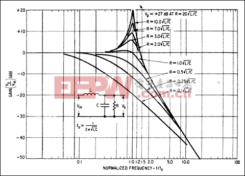
Figure 6. Amplitude characteristic for various damping ratios in the LC-Filter circuit of Figure 5.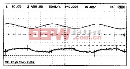
Figure 7. Input voltage and current ripple of LC-filter circuit (Figure 5). CIN = CFILTER = 100μF, and LFILTER = 10μH. Charge pump is MAX665. Input current ripple (upper trace): 100mA/div. Input voltage ripple (lower trace): 50mV/div, AC coupled.
3. Adding a low-dropout linear regulator to the charge pump's input supply (Figure 8) yields an effective general-purpose circuit for preventing the effects of ripple on the rest of the system. The input LDO also operates with smaller capacitors than those associated with a passive LC filter: the 300mA MAX8860 LDO (available in an 8-pin μMAX? package) requires 2.2μF capacitors at input and output; the MAX8863–MAX8864 family of 120mA linear regulators (available in SOT23 packages) requires only 1μF ceramic capacitors. The LDO must handle at least twice the charge pump's output load current, however. When compared with an equivalent passive filter, the added expense of that extra-current capability can place the LDO approach out of bounds in terms of cost and performance (pcb area and attenuation).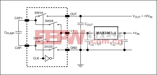
Figure 8. Charge pump doubler with LDO for input-ripple protection.
4. Adding an RC to the input supply (Figure 9) is a single-order version of the LC-filter approach. The RC input is not generally recommended, because the low value of RFILTER required for minimal efficiency loss ( 5Ω) forces a very large CFILTER. Figure 10 shows the effect of adding an RC filter at the input of the Figure 9 circuit, in which a MAX665 with 100μF capacitors generates a 5V output with a load resistance of 51Ω.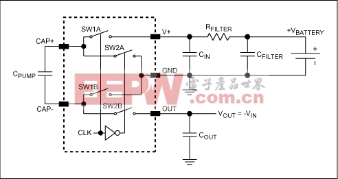
Figure 9. Battery application featuring a charge pump inverter with input RC ripple filter.
If the input supply is a battery, then the effective bulk capacitance of the battery can serve as CFILTER. Because CFILTER is a very large capacitance, the resulting filter is very effective in reducing ripple effects at the battery. An example helps to illustrate the point: the capacitance of an 800mAH Li cell can be derived from:
| Q = C.V | , where I = 800mA, T = 3600s (1Hr), and V = 3.4V. | |
| I.T = C.V |
Thus, C = 847 farads and fFILTER = 0.12mHz. The sum of ESR and battery contact resistance (about 100mΩ) limits the attenuation to a maximum of 21dB, assuming the ripple source resistance (RFILTER) equals 1Ω. The model for an actual battery is more complex, with the central bulk capacitance modified by ESR, ESL, and parasitic capacitance. In practice one should add capacitance close to RFILTER, thereby providing high frequency assistance and low ESR above 250kHz ( 50mΩ) to the battery and its interconnect leads. A typical value for the additional CFILTER is 470nF. For the MAX665 circuit of Figure 10, increasing CFILTER to 1500μF lowers the input voltage and current ripple as shown in Figure 11.
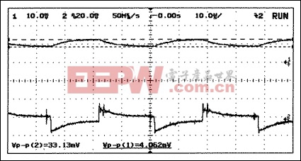
Figure 10. Input Voltage and Current Ripple for the RC-filter circuit (Figure 9): CIN = CFILTER = 100μF, and RFILTER = 2.2Ω. Charge pump is a MAX665. Input current ripple (upper trace): 100mA/div. Input voltage ripple (lower trace): 20mV/div, AC coupled.
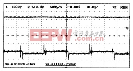
Figure 11. Input voltage and current ripple for the RC-filter circuit of Figure 7, with 1500μF quasi-battery capacitor: CIN =100μF, CFILTER = 1500μF, RFILTER = 2.2Ω, and MAX665 charge pump. Input current ripple (upper trace): 100mA/div. Input voltage ripple (lower trace): 20mA/div, AC coupled.
Conclusion
Several methods are available for reducing the effect of input power-supply ripple caused by charge pumps. Placing an LC filter in addition to the input capacitor recommended by the data sheet, for instance, (#2) provides excellent voltage-ripple protection to the rest of the system (Figure 10) with minimal effect on the overall conversion efficiency. An effective alternative for battery systems is a simple series resistor (#4), which occupies minimal space. The resistor is also suitable in non-battery applications for which large storage values (> 50μF) are appropriate. Results of a simulated battery application are shown in Figure 11.
An overview of Maxim's charge-pump ICs (Table 1) is included to help the reader choose an appropriate device according to the desired clock frequency, mode of operation, and level of output current required.
Table 1 Product Selection
| Package | 8-SO | 16-wSO | 8-μMax/SO | 8-μMax/SO |
| I/P Volts | 1.5V to 5.5V | 1.5V to 8V | 1.5V (inv) or 2.5V to 5.5V | 1.5V (inv) or 2.5V to 5.5V |
| O/P Current | 100mA | 100mA | 50mA | 50mA |
| Pump Rate | 10kHz/80kHz | 10kHz/45kHz | 3kHz/50kHz/130kHz | 13kHz/100kHz/250kHz |
| Mode | -VIN, +2VIN | -VIN, +2VIN | -VIN, +2VIN | -VIN, +2VIN |
| Regulated | No | No | No | No |
| Package | 8-SO | 8-SO | 5-SOT23 | 5-SOT23 |
| I/P Volts | 2.0V to 5.5V | 2.0V to 8V | 1.5V (inv) or 2.5V to 5.5V | 1.5V (inv) or 2.5V to 5.5V |
| O/P Current | 125mA | 125mA | 45mA | 45mA |
| Clock Freq | 125kHz/250kHz | 500kHz/1MHz | 12kHz | 35kHz |
| Mode | -VIN, +2VIN | -VIN, +2VIN | +2VIN | +2VIN |
| Regulated | No | No | No | No |
| Package | 5-SOT23 | 5-SOT23 | 6-SOT23 | 6-SOT23 |
| I/P Volts | 1.4V to 5.5V | 1.4V to 5.5V | 1.5V to 5.5V | 1.5V to 5.5V |
| O/P Current | 25mA | 25mA | 60mA | 25mA |
| Clock Freq | 125kHz | 500kHz | 12kHz/35kHz/125kHz/250kHz | 12kHz |
| Mode | -VIN | -VIN | -VIN | -VIN |
| Regulated | No | No | No | No |
| Package | 6-SOT23 | 16-QSOP | 8-μMax | 8-SO |
| I/P Volts | 1.5V to 5.5V | 2.0V to 6.0V | 1.5V to 6.0V | 2.0V to 6.0V |
| O/P Current | 25mA | ±10mA | ±10mA | ±10mA |
| Clock Freq | 125kHz | 7kHz/33kHz/100kHz/185kHz | 24kHz | 8kHz |
| Mode | -VIN | +2VIN and -VIN | +2VIN and -VIN | +2VIN and -VIN |
| Regulated | No | No | No | No |
| Package | 8-μMax | 8-SO | 8-μMax | 8-SO |
| I/P Volts | 2.0V to 3.6V | 4.5V to 5.5V | 1.8V to 3.6V | 2.7V to 5.5V |
| O/P Current | 60mA | 30mA | 20mA | 250mA |
| Clock Freq | 500kHz | 500kHz | 330kHz/1MHz | 200kHz/1MHz |
| Regulated | Yes | Yes | Yes | Yes |
| Package | 8-μMax | 8-μMax | 16-QSOP | 8-SO |
| I/P Volts | 2.7V to 5.5V | 2.7V to 5.5V | 3.0V to 5.5V | 2.5V to 10.0V |
| O/P Current | 100mA | 50mA | ±5mA | 4mA |
| Clock Freq | 5.0V | 5.0V | ±5V, Adj | -2.0V, Adj |
| Mode | 200kHz/1MHz | 200kHz/1MHz | 25kHz/100kHz, 20kHz-240kHz ext sync | 20kHz/100kHz |
| Regulated | Yes | Yes | Yes | Yes |
| Package | 8-SO | 10-μMax | 10-μMax | 8-SO |
| I/P Volts | 4.5V to 10.0V | 1.8V to 5.5V | 2.5V to 5.5V | 2.0V to 5.5V |
| O/P Current | 5mA | 30mA | 4mA | 125mA |
| O/P Volts | -4.1V, Adj | Adj, -2VIN max | -2V, Adj | Adj, -VIN max |
| Clock Freq | 100kHz 50kHz-250kHz ext sync | 450kHz | 100kHz | 350kHz |
| Regulated | Yes | Yes | Yes | Yes |
| Package | 8-μMax | 10-μMax | 8-μMax | |
| I/P Volts | 2.7V to 4.2V | 2.7V to 5.5V | 1.6V to 5.5V | |
| O/P Current | 12mA | 50mA | 100mA | |
| O/P Volts | 4.75V/5.0V | 1.8V/1.9V Adj | 3.3V, Adj | |
| Clock Freq | 1MHz | 450kHz | 1.5MHz | |
| Regulated | Yes | Yes | Yes |
μMAX is a registered trademark of Maxim Integrated Products, Inc.


評(píng)論