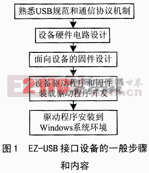
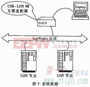
NXP LPC2468 USB接口解方案

NXP公司的LPC2468微控制器采用16位/32位ARM7TDMI-S CPU內(nèi)核,具有實時調(diào)試接口. LPC2468集成了高速512KB片內(nèi)閃存, 10/100以太網(wǎng)媒體接入控制器(MAC),帶4KB端點RAM的USB全速器件/主/OTG控制器,四個UART,兩個CAN通路和一些串行通信接口. LPC2468非常適合多用途的通信應用.本文介紹了LPC2468的主要特性,功能方框圖以及五種USB接口解決方案.
本文引用地址:http://www.104case.com/article/202335.htmNXP Semiconductors designed the LPC2468 microcontroller around a 16-bit/32-bit
ARM7TDMI-S CPU core with real-time debug interfaces that include both JTAG and
embedded trace. The LPC2468 has 512 kB of on-chip high-speed flash memory. This
flash memory includes a special 128-bit wide memory interface and accelerator
architecture that enables the CPU to execute sequential instructions from flash memory at
the maximum 72 MHz system clock rate. This feature is available only on the LPC2000
ARM microcontroller family of products. The LPC2468 can execute both 32-bit ARM and
16-bit Thumb instructions. Support for the two instruction sets means engineers can
choose to optimize their application for either performance or code size at the sub-routine
level. When the core executes instructions in Thumb state it can reduce code size by more than 30 % with only a small loss in performance while executing instructions in ARM state maximizes core performance.
The LPC2468 microcontroller is ideal for multipurpose communication applications. It
incorporates a 10/100 Ethernet Media Access Controller (MAC), a USB full-speed
Device/Host/OTG Controller with 4 kB of endpoint RAM, four UARTs, two Controller Area
Network (CAN) channels, an SPI interface, two Synchronous Serial Ports (SSP), three I2C interfaces, and an I2S interface. Supporting this collection of serial communications
interfaces are the following feature components; an on-chip 4 MHz internal precision
oscillator, 98 kB of total RAM consisting of 64 kB of local SRAM, 16 kB SRAM for
Ethernet, 16 kB SRAM for general purpose DMA, 2 kB of battery powered SRAM, and an
External Memory Controller (EMC). These features make this device optimally suited for
communication gateways and protocol converters. Complementing the many serial
communication controllers, versatile clocking capabilities, and memory features are
various 32-bit timers, an improved 10-bit ADC, 10-bit DAC, two PWM units, four external
interrupt pins, and up to 160 fast GPIO lines. The LPC2468 connects 64 of the GPIO pins
to the hardware based Vector Interrupt Controller (VIC) that means these external inputs
can generate edge-triggered interrupts. All of these features make the LPC2468
particularly suitable for industrial control and medical systems.
LPC2468主要特性:
ARM7TDMI-S processor, running at up to 72 MHz.
512 kB on-chip flash program memory with In-System Programming (ISP) and
In-Application Programming (IAP) capabilities. Flash program memory is on the ARM
local bus for high performance CPU access.
98 kB on-chip SRAM includes:
64 kB of SRAM on the ARM local bus for high performance CPU access.
16 kB SRAM for Ethernet interface. Can also be used as general purpose SRAM.
16 kB SRAM for general purpose DMA use also accessible by the USB.
2 kB SRAM data storage powered from the Real-Time Clock (RTC) power domain.
Dual Advanced High-performance Bus (AHB) system allows simultaneous Ethernet
DMA, USB DMA, and program execution from on-chip flash with no contention.
EMC provides support for asynchronous static memory devices such as RAM, ROM
and flash, as well as dynamic memories such as Single Data Rate SDRAM.
Advanced Vectored Interrupt Controller (VIC), supporting up to 32 vectored interrupts.
General Purpose AHB DMA controller (GPDMA) that can be used with the SSP,
I2S-bus, and SD/MMC interface as well as for memory-to-memory transfers.
Serial Interfaces:
Ethernet MAC with MII/RMII interface and associated DMA controller. These
functions reside on an independent AHB.
USB 2.0 full-speed dual port Device/Host/OTG Controller with on-chip PHY and
associated DMA controller.
Four UARTs with fractional baud rate generation, one with modem control I/O, one
with IrDA support, all with FIFO.
CAN controller with two channels.
SPI controller.
Two SSP controllers, with FIFO and multi-protocol capabilities. One is an alternate
for the SPI port, sharing its interrupt. SSPs can be used with the GPDMA controller.
Three I2C-bus interfaces (one with open-drain and two with standard port pins).
I2S (Inter-IC Sound) interface for digital audio input or output. It can be used with
the GPDMA.
Other peripherals:
SD/MMC memory card interface.
160 General purpose I/O pins with configurable pull-up/down resistors.


評論