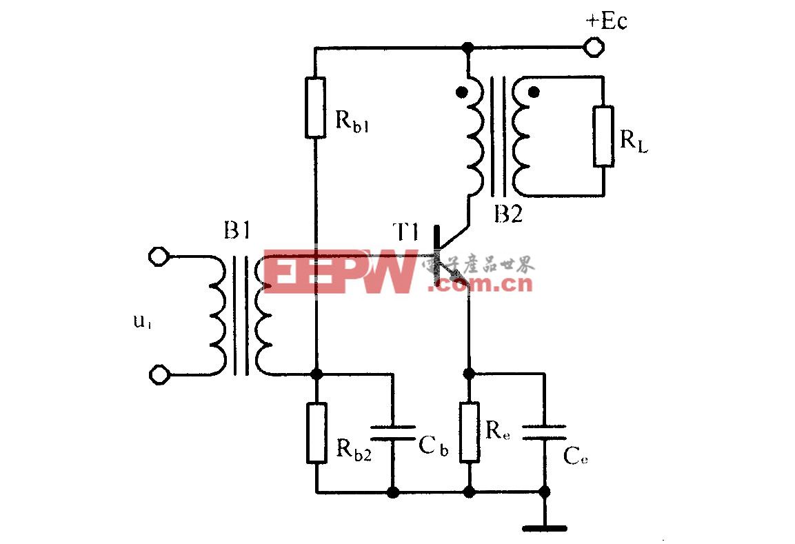
基于MC33905設計的MCU功率管理方案

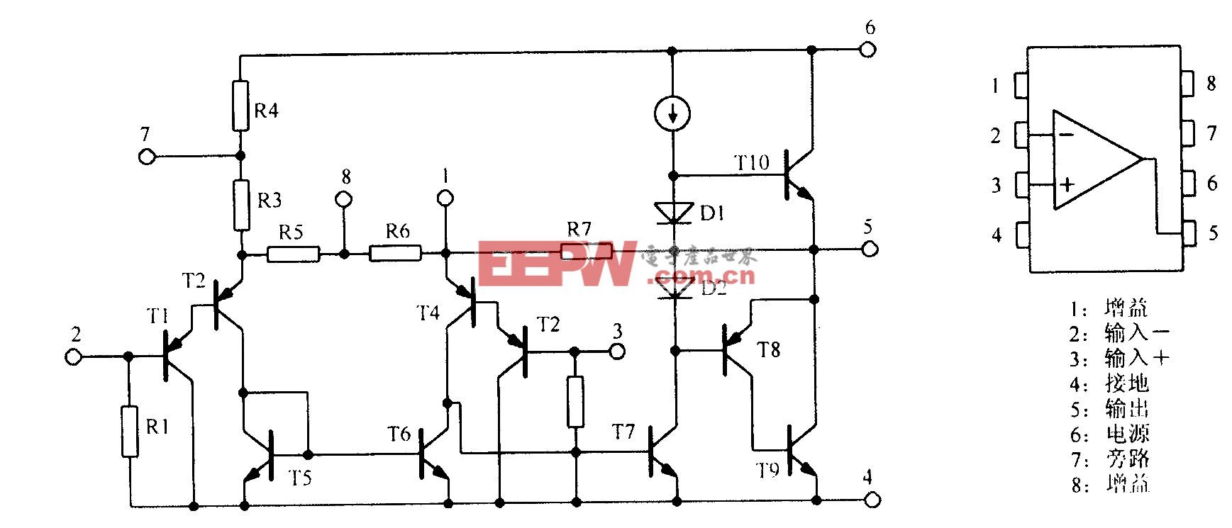
圖9.MC33905A典型應用電路圖
MC33905評估板EVB
This EVB includes two I/O test points that can be configured to be pulled up to VSup or pulled down to GND through a resistor and indicator LED. These are easily configured via jumper settings. The SBC can also be exercised in debug mode (watchdog re-fresh/monitoring not needed) by simply populating a jumper. Separating the input supply voltage to VSup1 and VSup2 is also made simple with a jumper configuration. Specified resistor pull-downs can be implemented on DBG and MUX pins via simple jumper configurations. The status of I/O0, I/O1, VAUX, 5V_CAN, SAFE and VDD can be visually monitored via on-board LEDs. The CAN and LIN Bus signals are provided through terminal block connectors.
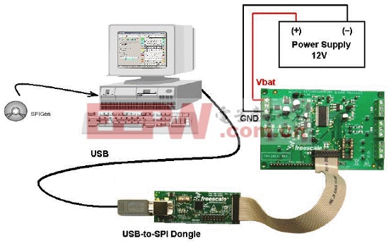
An isolated terminal block connector is implemented to provide power to the evaluation board with an external DC power supply.
The evaluation board is operated through the graphical user interface paired up with the SPI dongle board (KITUSBSPIDGLEVME) through the 2x8 pin ribbon cable. Additionally, for added flexibility, the user can implement a custom board with a microcontroller to talk to the SBC via the 16 pin header.
MC33905評估板EVB主要特性:
Nominal operating supply voltage range of 5.5V to 27V
Individually routed power supply inputs for VSup1 and VSup2
5.0 V regulator for MCU with external PNP ballast transistor to increase current capability.
Multiple CAN Bus termination options supported via socket
Two high/low side I/Os (SPI configurable) accessible through test points.
Status of I/O0 and I/O1 indicated by LED (dependent on jumper configuration)
Debug Mode/watchdog configuration via jumper settings
MUX output voltage accessible through test point and external resistor selectable through jumper
3.3 V or 5.0 V output voltage test point VAUX (SPI configurable)
I_WAKE_I test point to enable a FET and load VDD with current to wake up the SBC.
LIN1_T and LIN2_T test points to monitor I/O voltages (SPI configurable)
I/O0, I/O1, VAUX, 5V_CAN, SAFE and VDD status indicated by LED
100mil 2x8-pin standard header connector for SPI communication
100mil 16-pin standard header connector for custom MCU board connection
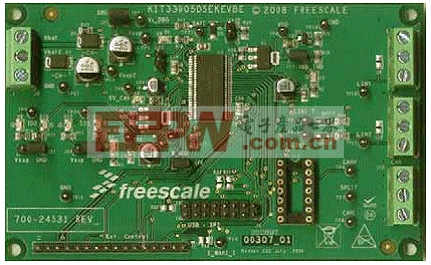
圖10.MC33905評估板KIT33905D5EKEVBE外形圖

評論