LED信號燈驅(qū)動器參考設(shè)計

Abstract: This application note presents a reference design for a signal-lamp linear LED driver that consists of six strings of 4 LEDs per string and delivers 350mA per string with a common cathode configuration. Common cathode arrangements require that the current-sense resistors be placed on the high (anode) side, which forces the LED drivers to use a level shifter.
Circuit Description
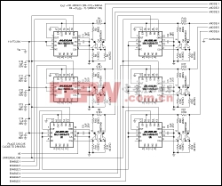
This application note describes a linear LED driver for six strings of 4 LEDs to be used in a signal lamp. The LED load provides independent access to the anodes of each string, but the cathodes are common connected. The circuit operates from an automotive battery with a minimum voltage of 10V and a maximum of 28V, while delivering 350mA to each string.
Because of the common cathode configuration, the current-sense resistors must be located on the anode side of the LED strings. Since the LED driver's (MAX16836) current-sense inputs are limited to 4V of common-mode voltage, the voltage across the sense resistors must be level shifted and ground referenced to be compatible with the drivers. The PNP transistor pairs translate the voltage across the LED current-sense resistor to a GND-referenced voltage that is fed into the current-sense pin of the MAX16836. The following equations provide the values for R1, R2, R3, and R4 (in the U1 section of the schematic):
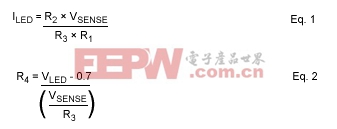
Where VSENSE is the current-sense voltage of the IC (200mV).
When the LED string is at its minimum voltage (7.6V) and the input is at its maximum (28V), the LED drivers experience losses of over 7W. Dissipating this heat is almost impossible with circuit board heatsinking methods, so at high voltages a dimming signal with reduced duty cycles (down to 25%) drives the UNIVERSAL DIM input to lessen the power dissipation in the drivers.
This reference design allows for independent enables that allow each string to be controlled separately.
Figure 1 presents a schematic for the circuit, and Table 1 provides the Bill of Materials (BOM). The following are the electrical input requirements and output capabilities.
VIN: 11V to 28V
PWMIN: 10% to 100%
VLED configuration: 7.6VDC (min) to 10VDC (max), 350mA
More detailed image (PDF, 7.96kB)
Figure 1. Schematic of the driver design.
Table 1. Bill of Materials


評論