于C8051F99x設計的低功耗高靈敏容性觸摸技術

25 MIPS, 8 kB Flash, Ultra Low Power, Capacitive Sensing MCU
The QuickSense? C8051F99x family of capacitive sensing MCUs provides the lowest power and highest sensitivity touch sensing solution for capacitive buttons, sliders, wheels and capacitive proximity sensing. Architected from the popular C8051F9xx platform the device features a 150 μA/MHz active mode and multiple sleep modes as low as 10 nA. With up to 14 capacitive sensing inputs and a patent-pending charge timing hardware capacitance to digital converter, the C8051F99x achieves unparalleled touch sensitivity, speed and ultra-low power in packages as small as a 3 mm x 3 mm QFN20.
C8051F99x系列主要特性:
Capacitance to Digital Converter
-Supports buttons, sliders, wheels, and capacitive proximity sensing
-Fast 40 μs per channel conversion time
-16-bit resolution
-Up to 14 input channels
-Auto-accumulate up to 64x samples
Ultra-Low Power
-150 μA/MHz active current from 1.8–3.6 V @ 25 MHz
-10 nA sleep current with data retention; BOD disabled
-50 nA sleep current with data retention; BOD enabled
-300 nA sleep current with smaRTClock (internal oscillator)
-600 nA sleep current with smaRTClock (external crystal)
-2 μs wake up from sleep
Supply Voltage 1.8 to 3.6 V
-Built-in brown-out detector
-On-chip LDO regulator for core supply
Analog to Digital Converter
-75 ksps with 12-bit resolution (F990/6)
-330 ksps with 8-bit resolution
-Up to 10-channels
-Autonomous burst mode with 16-bit averaging accumulator
-VREF from external pin, VDD, or internal regulator
-Built-in temperature sensor
Internal 6-Bit Current Reference
-2 ranges: source or sink capability
-Up to 14-bit resolution via PWM interpolation
Comparator
-Programmable hysteresis and response time
-Configurable as interrupt or reset source
-Low current ( 0.4 μA)
Development Kit: C8051F996DK
High-Speed 8051 μC Core
-Pipe-lined instruction architecture; executes 70% of instructions in 1 or 2 system clocks
-25 MIPS peak throughput with 25 MHz clock
-Expanded interrupt handler
Memory
-512 bytes internal data RAM (256 + 256)
-8 kB Flash; In-system programmable in 512 byte sectors; Full read/write/erase functionality over the entire supply range
On-Chip Debug
-On-chip debug circuitry facilitates full speed, non-intrusive in-system debug
Digital Peripherals
-17 port I/O; Programmable drive strength
-Hardware enhanced UART, SPI and SMBus? serial ports
-CRC block provides 16-Bit CCITT polynomial calculation
-Four general purpose 16-bit counter/timers
-16-bit programmable counter array (PCA) with three capture/compare modules and enhanced PWM functionality
Clock Sources
-24.5 MHz ±2% oscillator; supports crystal-less UART operation
-Low power internal oscillator: 20 MHz
-External oscillator: Crystal, RC, C, CMOS clock
-Can switch clock sources on-the-fly; useful for power saving modes
Temperature Range: -40 to +85 °C
Package Options
-24-pin QFN (4x4 mm), RoHS compliant
-24-pin QSOP (easy to hand solder) RoHS compliant
-20-pin QFN (3x3 mm), RoHS compliant
C8051F99x 應用:
Instrumentation panels
Touch panels
Kiosks
Gaming systems
Industrial interface
Security
Residential HVAC
Home appliances
Toys
Keyboards
Fax/printer/scanner front panels
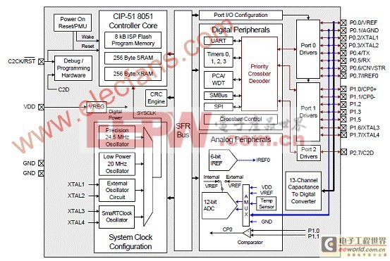
圖1。C8051F990方框圖
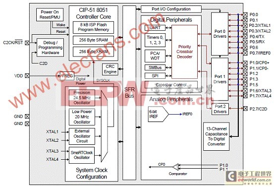
圖2。C8051F991方框圖
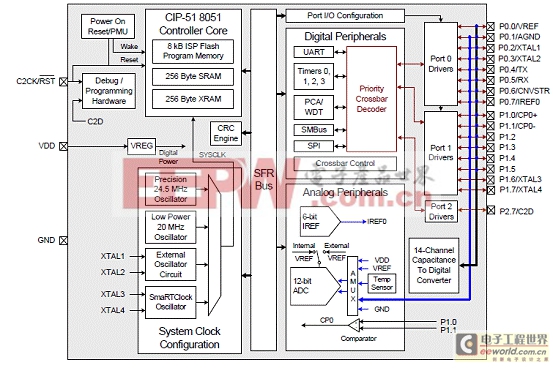
圖3。C8051F996方框圖
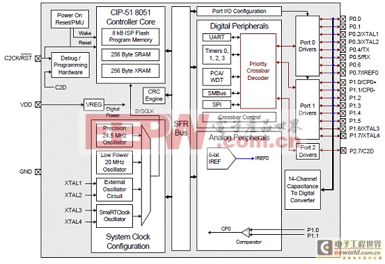
圖4。C8051F997方框圖
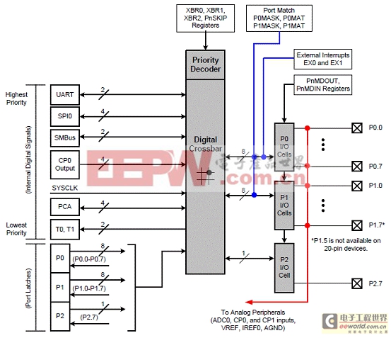
圖5。C8051F99x系列I/O端口功能方框圖
C8051F996 開發套件
The C8051F996DK Development Kit contains everything needed to develop applications with the C8051F990, F991, F996 and F997 family ofultra low powercapacitive sensing MCUs and the C8051F980, F981, F982, F983, F985, F986, F987, F988 and F989 family of ultra low power MCUs.
The C8051F996 Development Kit contains the following items:
? C8051F996 Target Board
? C8051Fxxx Development Kit Quick-Start Guide
? Silicon Laboratories IDE and Product Information CD-ROM. CD content includes the following:
??Silicon Laboratories Integrated Development Environment (IDE)
??Evaluation version of 8051 development tools (macro assembler, linker, C compiler)
??Source code examples and register definition files
??Documentation
??C8051F996 Development Kit User’s Guide (this document)
? Third Party Tools CD
? AC to DC Power Adapter
? USB Debug Adapter (USB to Debug Interface)
? 2 USB Cables
? 2 AAA Batteries
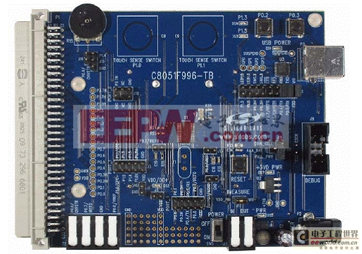
圖6。C8051F996 目標板外形圖
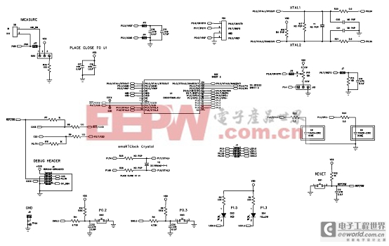
圖7。C8051F996 目標板電路圖(1)

圖8。C8051F996 目標板電路圖(2)
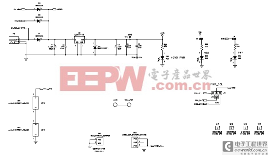
圖9。C8051F996 目標板電路圖(3)

評論