電壓型逆變器集成電路形式高效軌道器-Voltage-Inve

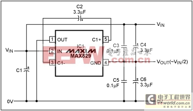
Figure 1. This compact and efficient charge-pump circuit implements a local dual-rail supply for single-rail systems.
After power is applied, the flying capacitor (C2) connects alternately across the storage capacitors C3/C4 and C5/C6. This action equalizes the voltages on those capacitors and draws current from VIN or VOUT as required to maintain VOUT ≈ ?VIN.
If the loads across VIN-VOUT and VOUT-0V are equal, the IC sits in a quiescent state and draws about 36μA. To keep VOUT at the mid-rail level, the flying capacitor needs only to supply the difference current caused by unbalanced loads. Efficiency is degraded by the IC's quiescent current for load currents below 100μA, but above 1mA the efficiency is greater than 90%—an excellent feature for low-power or battery-powered applications. (Voltage error and efficiency vary with the load current, as shown in Figures 2 and 3.)
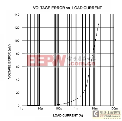
Figure 2. The output voltage error in Figure 1 increases with load current.
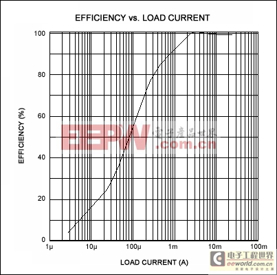
Figure 3. Efficiency also increases with load current in Figure 1.
This switched-capacitor circuit provides better regulation than that of a simple voltage divider, and better efficiency than that of a simple combination of divider and op-amp buffer. Its main drawback is the increase in output noise with load (see Table 1). VIN is restricted (by the IC specifications) to a maximum of 5.5V, which is the maximum voltage allowed between pins 2 and 4 or between pins 1 and 4.
| RLOAD (Ω) | INPUT CURRENT (μA) | VOUT ERROR (mV) | OUTPUT CURRENT (μA) | RIPPLE (mVP-P) | EFFICIENCY (%) |
| ∞ | 36.5 | — | — | — | — |
| 10M | 36.5 | — | 0.25 | — | 0.34 |
| 10M | 37.7 | — | 2.5 | — | 3.32 |
| 100k | 48.9 | 0.1 | 25 | — | 25.56 |
| 10k | 156 | 1.4 | 250 | ~1 | 80.04 |
| 1k | 1240 | 13.5 | 2490 | ~5 | 99.72 |
| 470 | 2630 | 28.5 | 5260 | ~8 | 98.83 |
| 100 | 11,410 | 126.9 | 23,700 | ~30 | 98.71 |
A similar idea appeared in the August 1, 1997 issue of EDN.


評論