建立快速電壓瞬態(tài)-Creating Fast Line Tr

One solution to obtaining this fast transient into large capacitive loads is to make an open-loop buffer. Because an open-loop buffer has no feedback, it is insensitive to capacitive loads and can be designed to meet most current requirements. Important criteria for this buffer include high slew rate, high output drive, low offset voltage, low distortion, and thermal compensation.
The circuit in the figure below satisfies these requirements. It is similar to the classic BJT buffer with a few modifications. Because the transistors used are not on a single monolithic die, some means has to be provided to adjust the bias. Furthermore, the circuit must have some method to keep this bias constant over temperature.

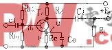
Figure 1. Open-loop buffer schematic.
The circuit consists of three major blocks. There is a high-impedance complementary input stage, followed by a VBE multiplier for bias adjustment, and then a complementary Darlington output stage. The input stage and the VBE multiplier are biased with constant current sources, whereas the output stage is biased by the output of the VBE multiplier.
The key to connecting the input stage to the VBE multiplier and the output stage is the inclusion of some series resistance via resistors R7 and R8. This allows the VBE multiplier to control the output stage bias without fighting the bias levels of the input stage. This becomes a factor as the output stage heats up due to load requirements. If the series resistors were not included, the input stage would overbias the output stage at elevated temperatures. Because the VBE multiplier is mounted on the output heatsink, it thermally tracks the output stage, eliminating thermal runaway.
This circuit is designed for bipolar power supplies above the maximum output by about 5V and below the minimum output by about 5V. Operation at +15V and -5V provides good performance. Note that multiple grounds have been included on the board. The input supplies should use a short pair of heavy-gauge wire to the PCB. Do not share these grounds with any other circuitry. The output should be connected to the DUT input with very short heavy-gauge wires. These wires will carry transient currents in excess of 10A and should be sized accordingly.
The buffer was designed with a high input impedance to have flexible drive requirements. Don't connect the output of the buffer to the input of the DUT without a driving signal on the buffer input. If the output voltages are under ±5V, use a 50Ω terminator right at the buffer input. If the output is up to 10V, run the pulse generator unterminated to get this voltage. Voltages beyond this will require the addition of an external amplifier. The maximum supply voltages for the buffer are |V+ - V-| 40V.


評論