保護(hù)電流檢測(cè)放大器反對(duì)過壓瞬變-Protect Curren

A similar article appeared in the October 25, 2007 issue of Electronic Design.
Some current-sense amplifiers encounter overvoltages frequently. A current-sense amplifier that monitors battery-discharge currents in an automobile, for example, must withstand the high-voltage load-dump pulses produced when loads are disconnected from the battery, causing inductive spikes and overvoltages to appear at the output of the alternator. If these pulses exceed the amplifier's common-mode voltage, then one must provide external circuitry to protect the amplifier.
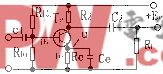
Figure 1 shows an example of a protection circuit, which is composed of zener diodes Z1 and Z2, resistors R1 and R2, and diode D1. The common-mode voltage range of the MAX4372 amplifier is 0 to 28V, which is more than sufficient for measuring automotive battery voltages that vary from 6V to 18V. Load-dump voltages, however, can reach 35V and persist for 0.5 seconds, which is well over the amplifier's 30V absolute maximum rating for input voltage. The amplifier must therefore be well-protected externally.
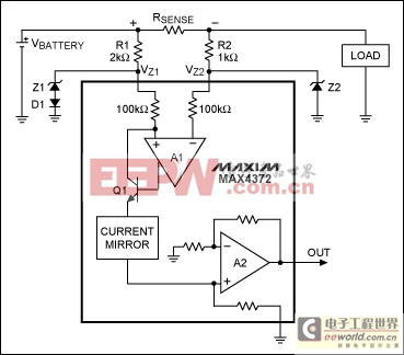
Figure 1. This current-sense amplifier has protection circuitry (upper circuit components) suitable for common-mode voltages above 30V.
You can avoid additional errors in the input offset voltage by using different values for the input-protection resistors R1 and R2 (2kΩ and 1kΩ, respectively), thereby balancing the effect of the amplifier's unequal bias currents. For selection of these resistor values, refer to the application note 3888, "Performance of Current-Sense Amplifiers with Input Series Resistors."
Zener diodes Z1 and Z2 have nominal breakdown voltage of 24V, and are chosen to have sufficient power-dissipation capability to withstand the ~11mA sink currents that flow during a 35V peak load-dump condition (the 35V load-dump voltage minus a 24V clamp voltage appears across the 1kΩ series resistor R2).
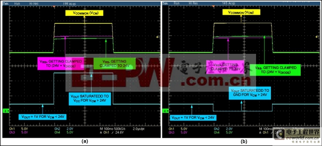
Figure 2 depicts the amplifier output in the presence of 35V load-dump pulses with D1 removed. With normal battery voltages applied, the 1V output value is as expected (input VSENSE = 50mV, and gain = 20). When a load-dump voltage appears, the zeners clamp the input common-mode voltage to about 24V, and the amplifier output makes a few transient excursions before settling down to 0V.
Figure 2. Operation of the Figure 1 circuit with diode D1 removed.
Though nominally 24V, the two zeners generally have slightly different breakdown voltages due to part-to-part variations and different operating currents (Z1 operates at 5.5mA and Z2 operates at 11mA). Therefore, the quantity (VZ1 - VZ2) appears as a changing differential sense voltage causing unwanted output transients. If desired, you can eliminate these transients by adding a diode in series with either Z1 or Z2. The diode forces (VZ1 - VZ2) to be either positive or negative during a load-dump condition, which in turn forces the amplifier output to one of the supply rails (VCC or GND), and thereby preventing random output response during an input transient.
Figure 3a shows the circuit operating with the diode connected in series with Z1, which forces the amplifier output to the positive rail. Figure 3b shows the diode connected in series with Z2, which forces the amplifier output to the negative rail.
More detailed image (PDF, 892kB)
Figure 3. Operation of the Figure 1 circuit with D1 in series with Z1 (a), and D1 in series with Z2 (b).


評(píng)論