ARM協處理器CP15設置MMU,cache等學習

協處理器CP15包含了如下寄存器。
本文引用地址:http://www.104case.com/article/201611/318747.htm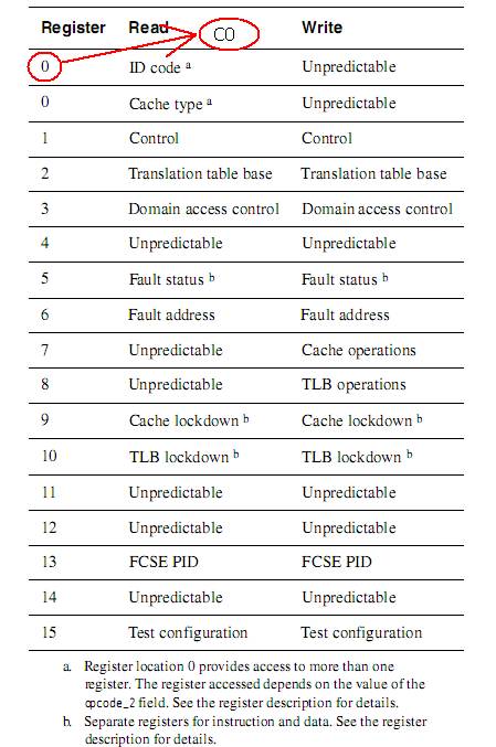
========================================================================
在ARM920T Technical Reference Manual中有如下關鍵術語
2.3.1 Addresses in ARM920T
Three distinct types of address exist in an ARM920T system:
• Virtual Address (VA)
• Modified Virtual Address (MVA)
• Physical Address (PA).
Below is an example of the address manipulation when the ARM9TDMI core requests
an instruction (see Figure 2-10 on page 2-25).
1. The Instruction VA (IVA) is issued by the ARM9TDMI core.
2. This is translated by the ProcID to the Instruction MVA (IMVA). It is the IMVA
that the Instruction Cache (ICache) and MMU see.
3. If the protection check carried out by the IMMU on the IMVA does not abort, and
the IMVA tag is in the ICache, the instruction data is returned to the ARM9TDMI
core.
4. If the ICache misses (the IMVA tag is not in the ICache), then the IMMU
performs a translation to produce the Instruction PA (IPA). This address is given
to the AMBA bus interface to perform an external access.
_________________________________________________這些東西我就不具體翻譯了,免得誤人子弟。
2.3.2 Accessing CP15 registers訪問CP15 寄存器
The terms and abbreviations(縮寫詞) shown in Table 2-4 are used throughout this section.
Table 2-4 CP15 abbreviations
Term Abbreviation Description
UnpredictableUNP
For reads, the data returned when reading from this location is unpredictable. It can
have any value.
For writes, writing to this location causes unpredictable behavior, or an unpredictable
change in device configuration.
Should be zeroSBZ
When writing to this location, all bits of this field should be 0.
————————————————————————————————————————
You can only access CP15 registers with MRC and MCR instructions in aprivileged mode.(特權模式)
MCR/MRC{cond} P15,opcode_1,Rd,CRn,CRm,opcode_2
————
Instructions CDP, LDC, and STC, together with unprivileged MRC and MCR instructions to CP15, cause the undefined instruction trap to be taken(導致未定義...).The CRn field of MRC and MCR instructions specifies the coprocessor register to access.The CRm field and opcode_2 fields specify a particular action when addressing registers. The L bit distinguishes between an MRC (L=1) and an MCR (L=0).——指明了CRn 和CRm 的作用。
————
Note
Attempting to read from a nonreadable register, or to write to a nonwritable register causes unpredictable results.
Theopcode_1, opcode_2, and CRmfields should be zero, except when the values specified are used to select the desired operations, in all instructions that access CP15. Using other values results in unpredictable behavior.
——這里用意何在?等到下面看看代碼才知道。
————————————————————————————————————————
Register 0, ID code register(讀芯片32位ID)
This is a read-only register that returns a 32-bit device ID code.
You can access the ID code registerby reading CP15 register 0 with the opcode_2 field set to any value other than 1 (the CRm field should be zero when reading).For example:
MRC p15,0,Rd,c0,c0,0 ; returns ID register
——芯片ID代表含義
Table 2-5 Register 0, ID code
Register bits FunctionValue
31:24 ——Implementer0x41——這個是什么意思?
23:20—— Specification revision0x1
19:16 ——Architecture (ARMv4T)0x2
15:4—— Part number0x920
3:0 ——Layout revision Revision
————————————————————————————————————————
2.3.4 Register 0, cache type register
This is a read-only register that contains information about the size and architecture of
the caches, allowing operating systems to establish how to perform such operations as
cache cleaning and lockdown. All ARMv4T and later cached processors contain this
register, allowing RTOS vendors to produce future-proof versions of their operating
systems.
You can access the cache type register by reading CP15 register 0 with theopcode_2 field
set to 1. For example:
MRC p15,0,Rd,c0,c0,1 ; returns cache details

評論