STM32_GPIO配置及庫函數講解——獨立按鍵

LED硬件連接如下圖所示:高電平點亮LED。
本文引用地址:http://www.104case.com/article/201611/318316.htm
要想將PB9管腳配置成輸入模式,程序所需如下步驟:(必須的)
第一步:配置系統時鐘。見STM32F103xRCC寄存器配置
除此之外,還需將GPIO外設時鐘打開。
/* Enable GPIOC and GPIOB clock */
RCC_APB2PeriphClockCmd(RCC_APB2Periph_GPIOB,ENABLE);
RCC_APB2PeriphClockCmd(RCC_APB2Periph_GPIOC,ENABLE);
第二步:配置中斷向量表。決定將程序下載到RAM中還是FLASH中。以后講。
voidNVIC_Configuration(void)
{
#ifdefVECT_TAB_RAM
/* Set the Vector Table base location at 0x20 */
NVIC_SetVectorTable(NVIC_VectTab_RAM,0x0);
#else/* VECT_TAB_FLASH */
/* Set the Vector Table base location at 0x08 */
NVIC_SetVectorTable(NVIC_VectTab_FLASH,0x0);
#endif
}
第三步:配置GPIO的模式。輸入模式還是輸出模式。STM32_GPIO配置及庫函數講解——LED跑馬燈已講過。
void GPIO_Configuration(void){GPIO_InitTypeDef GPIO_InitStructure;/* Configure PC.06, PC.07, PC.08 and PC.09 as Output push-pull */GPIO_InitStructure.GPIO_Pin = GPIO_Pin_6 GPIO_Pin_7 GPIO_Pin_8 GPIO_Pin_9;GPIO_InitStructure.GPIO_Speed = GPIO_Speed_50MHz;GPIO_InitStructure.GPIO_Mode = GPIO_Mode_Out_PP; GPIO_Init(GPIOC, &GPIO_InitStructure);/* Configure PB.09 as Input pull-up */GPIO_InitStructure.GPIO_Pin = GPIO_Pin_9;GPIO_InitStructure.GPIO_Mode = GPIO_Mode_IPU; //上拉輸入GPIO_Init(GPIOB, &GPIO_InitStructure);}第四步:讀該管腳上的電平狀態。需要介紹一個庫函數。
vGPIO_ReadInputDataBit從指定Port指定Pin,讀該管腳上的電平狀態:
u8 GPIO_ReadInputDataBit(GPIO_TypeDef*GPIOx,u16 GPIO_Pin)
{
u8 bitstatus=0x00;
/* Check the parameters */
assert_param(IS_GPIO_ALL_PERIPH(GPIOx));
assert_param(IS_GET_GPIO_PIN(GPIO_Pin));
if((GPIOx->IDR&GPIO_Pin)!=(u32)Bit_RESET)
{
bitstatus=(u8)Bit_SET;
}
else
{
bitstatus=(u8)Bit_RESET;
}
returnbitstatus;
}
涉及到GPIO_IDR寄存器,如下所示
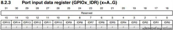

經過上面4步,就可以檢測PB9管腳的電平狀態。
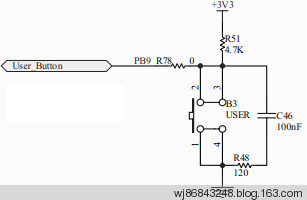
按鍵按下,PB9管腳應該是低電平,怎么才能驗證,最簡單的方法是:當按鍵被按下,點亮所有LED。
下面給出完整程序:
/* Includes */
#include"stm32f10x_lib.h"
/* Private function prototypes --*/
voidRCC_Configuration(void);
voidNVIC_Configuration(void);
voidGPIO_Configuration(void);
voidDelay(vu32 nCount);
/*******************************************************************************
* Function Name : main
* Description : Main program.
* Input : None
* Return : None
*******************************************************************************/
intmain(void)
{
#ifdefDEBUG
debug();
#endif
/* Configure the system clocks */
RCC_Configuration();
/* NVIC Configuration */
NVIC_Configuration();
/* Configure the GPIO ports */
GPIO_Configuration();
/* Infinite loop */
while(1)
{
if(GPIO_ReadInputDataBit(GPIOB,GPIO_Pin_9)==0)//檢測USR鍵是否被按下,若按下,則點亮全部LED
{
GPIO_SetBits(GPIOC,GPIO_Pin_6GPIO_Pin_7GPIO_Pin_8GPIO_Pin_9);
}
else
{
GPIO_ResetBits(GPIOC,GPIO_Pin_6GPIO_Pin_7GPIO_Pin_8GPIO_Pin_9);
}
}
}
/*******************************************************************************
* Function Name : RCC_Configuration
* Description : Configures the different system clocks.
* Input : None
* Return : None
*******************************************************************************/
voidRCC_Configuration(void)
{
ErrorStatusHSEStartUpStatus;
/* RCC system reset(for debug purpose) */
RCC_DeInit();
/* Enable HSE */
RCC_HSEConfig(RCC_HSE_ON);
/* Wait till HSE is ready */
HSEStartUpStatus=RCC_WaitForHSEStartUp();
if(HSEStartUpStatus==SUCCESS)
{
/* Enable Prefetch Buffer */
FLASH_PrefetchBufferCmd(FLASH_PrefetchBuffer_Enable);
/* Flash 2 wait state */
FLASH_SetLatency(FLASH_Latency_2);
/* HCLK = SYSCLK */
RCC_HCLKConfig(RCC_SYSCLK_Div1);
/* PCLK2 = HCLK */
RCC_PCLK2Config(RCC_HCLK_Div1);
/* PCLK1 = HCLK/2 */
RCC_PCLK1Config(RCC_HCLK_Div2);
/* PLLCLK = 8MHz * 9 = 72 MHz */
RCC_PLLConfig(RCC_PLLSource_HSE_Div1,RCC_PLLMul_9);
/* Enable PLL */
RCC_PLLCmd(ENABLE);
/* Wait till PLL is ready */
while(RCC_GetFlagStatus(RCC_FLAG_PLLRDY)==RESET){}
/* Select PLL as system clock source */
RCC_SYSCLKConfig(RCC_SYSCLKSource_PLLCLK);
/* Wait till PLL is used as system clock source */
while(RCC_GetSYSCLKSource()!=0x08){}
}
/* Enable GPIOC and GPIOB clock */
RCC_APB2PeriphClockCmd(RCC_APB2Periph_GPIOB,ENABLE);
RCC_APB2PeriphClockCmd(RCC_APB2Periph_GPIOC,ENABLE);
}
/*******************************************************************************
* Function Name : NVIC_Configuration
* Description : Configures Vector Table base location.
* Input : None
* Return : None
*******************************************************************************/
voidNVIC_Configuration(void)
{
#ifdefVECT_TAB_RAM
/* Set the Vector Table base location at 0x20 */
NVIC_SetVectorTable(NVIC_VectTab_RAM,0x0);
#else/* VECT_TAB_FLASH */
/* Set the Vector Table base location at 0x08 */
NVIC_SetVectorTable(NVIC_VectTab_FLASH,0x0);
#endif
}
/*******************************************************************************
* Function Name : GPIO_Configuration
* Description : Configures the different GPIO ports.
* Input : None
* Return : None
*******************************************************************************/
voidGPIO_Configuration(void)
{
GPIO_InitTypeDef GPIO_InitStructure;
/* Configure PC.06, PC.07, PC.08 and PC.09 as Output push-pull */
GPIO_InitStructure.GPIO_Pin=GPIO_Pin_6GPIO_Pin_7GPIO_Pin_8GPIO_Pin_9;
GPIO_InitStructure.GPIO_Speed=GPIO_Speed_50MHz;
GPIO_InitStructure.GPIO_Mode=GPIO_Mode_Out_PP;
GPIO_Init(GPIOC,&GPIO_InitStructure);
/* Configure PB.09 as Input pull-up */
GPIO_InitStructure.GPIO_Pin=GPIO_Pin_9;
GPIO_InitStructure.GPIO_Mode=GPIO_Mode_IPU;//上拉輸入
GPIO_Init(GPIOB,&GPIO_InitStructure);
}
/*******************************************************************************
* Function Name : Delay
* Description : Inserts a delay time.
* Input : nCount: specifies the delay time length.
* Return : None
*******************************************************************************/
voidDelay(vu32 nCount)
{
for(;nCount!=0;nCount--);
}
#ifdefDEBUG
/*******************************************************************************
* Function Name : assert_failed
* Description : Reports the name of the source file and the source line number
* where the assert_param error has occurred.
* Input : - file: pointer to the source file name
* - line: assert_param error line source number
* Return : None
*******************************************************************************/
voidassert_failed(u8*file,u32 line)
{
/* User can add his own implementation to report the file name and line number,
ex: printf("Wrong parameters value: file %s on line %drn", file, line) */
/* Infinite loop */
while(1)
{
}
}
#endif
還有個問題:PB9的初始狀態是什么?或者說GPIO_Configuration函數后PB9管腳上是高電平還是低電平?
這要看GPIO_InitStructure結構體的GPIO_Mode成員變量初始化為什么,如果為上拉,則PB9管腳為高電平;如果為下拉,則PB9管腳為低電平。
GPIO管腳內部電路設計如圖:
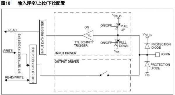
當GPIO初始化為輸入上拉模式,由上圖可知:該端口向外輸出高電平,即:ODR對應位為1
當GPIO初始化為輸入下拉模式,由上圖可知:該端口向外輸出低電平,即:ODR對應位為0
如何調試:在下面兩處處設個斷點。
1. GPIO初始化函數GPIO_Configuration中
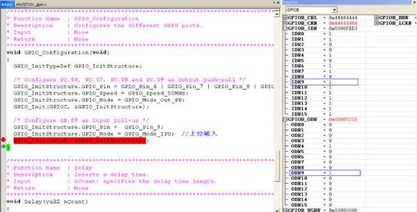
可以看到:當GPIO設置成輸入上拉模式時,等待GPIO初始化完畢,該管腳ODR9為1
2. 在main函數中,設置一個斷點。
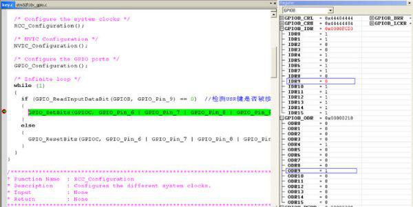
全速執行(F5),按住UserButton不放,可以看到GPIOB_IDR的IDR9=0。當放開按鍵時,再單步調試(F10),
GPIOB_IDR的IDR9=1。

評論