深入理解ARM體系架構(S3C6410)---S3C6410系統時鐘

在電源控制邏輯中,S3C6410 有多種電源管理方案,以保持電力系統的最佳消耗。In the power control logic, S3C6410X has various power managementschemes to keep optimal power consumption for a given task.
1、在S3C6410中,通用時鐘門控模式用來控制內部外設時鐘的開/關。可以通過用于外設所要求的特定應用提供時鐘,使用通用時鐘門控模式來優化S3C6410的電源消耗。例如:如果定時器沒有要求,則可以中斷時鐘定時器,以降低功耗。General Clock Gating mode is used to control the ON/OFF of clocksfor internal peripherals in S3C6410X. You can optimize the power consumption ofS3C6410X using this General Clock Gating mode by supplying clocks for peripheralsthat are required for a certain application. For example, if a timer is notrequired, then you can disconnect the clock to the timer to reduce power.
2、閑置模式僅中斷ARMCLK到CPU 內核,它提供時鐘給所有外設。通過使用閑置模式,電力消耗通過CPU
內核而減少。
3、停止模式通過禁用PLL凍結所有時鐘到CPU 以及外設。在S3C6410 中,電力消耗僅因為漏電流。
4、睡眠模式斷開內部電源。因此,除了喚醒邏輯單元消耗的電量,CPU和內部邏輯消耗電量將為零。為了使用睡眠模式,兩個獨立的電源是必需的。其中一個電源為喚醒邏輯提供電力,另一個提供其他內部邏輯,包括CPU。SLEEP mode disconnects the internal power.Therefore, the power consumption due to CPU and the internal logic except thewakeup logic will be zero. In order to use the SLEEP mode two independent powersources are required. One of the two power sources supplies the power for thewake-up logic. The other one supplies the other internal logic including CPU,and must be controlled in order to be turned ON/OFF. In SLEEP mode, the secondpower supply source for the CPU and internal logic will be turned off.
3.1 系統控制器的特性
The System Controller includes the following features:
• Three PLLs: ARM PLL, main PLL, extra PLL (for the modules those usespecial frequency)
• Five power-saving mode: NORMAL, IDLE, STOP, DEEP-STOP, and SLEEP
• Six controllable power domain: domain-G, domain-V, domain-I,domain-P, domain-F, domain-S
• Control operating clocks of internal sub-blocks
• Control bus priority
3.2 功能描述
這部分主要介紹S3C6410 系統控制器的功能。包含時鐘的體系結構,復位設計和電源管理模式。
1、硬件結構
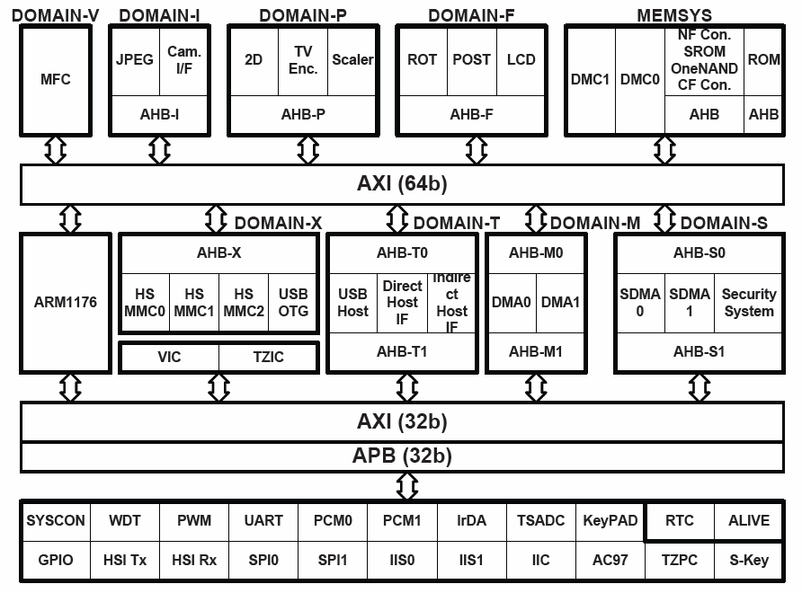
S3C6410是由ARM1176核、一些多媒體協處理器(co-processors)、多種外設IPs組成。ARM1176核是通過64位AXI總線與存儲控制器相連的,這樣做是為了滿足帶寬的需要。多媒體協處理(MFC多格式編碼器、JPEG、camera接口、TV譯碼器、3D加速器等)器被分為五個電源域,這五個電源域可被單獨控制以降低功耗。S3C6410X consists of ARM1176 processor, several media and graphicco-processors and various peripheral IPs. ARM1176 processor is connected toseveral memory controllers through 64-bit AXI-bus. This is done to meetbandwidth requirements. Media and graphic coprocessors, which include MFC(Multi-Format Codec), JPEG, Camera interface, TV encoder, 3D accelerator and etc,are divided into six power domains. The six power domain can be controlledindependently to reduce unwanted power consumption when the IPs is not requiredfor an application program.
2、時鐘結構
時鐘源在外部晶振和外部時鐘二者之間進行選擇。時鐘發生器由三個PLL組成,最高可產生1.6GHz的信號。
3.時鐘源的選擇
The OM[4:0] pins determines theoperating mode of S3C6410X when the external reset signal is asserted. Asdescribed in the table, the OM[0] selects the external clock source, i.e., ifthe OM[0] is 0, the XXTIpll (external crystal) is selected.
Otherwise, XEXTCLK is selected.
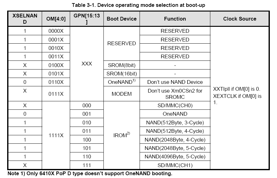
The operating mode is mainlyclassified into six categories according to the boot device. The boot devicecan be among SROM, NOR, OneNAND, MODEM and Internal ROM. When NAND Flash deviceis used, XSELNAND pin must be 1, even if it is used as boot device or storagedevice. When OneNAND Flash device is used, XSELNAND must be 0, even if it isused as boot device or storage device. When NAND/OneNAND device is not used,
XSELNAND can be 0 or 1.
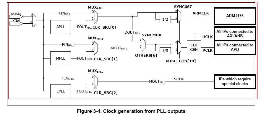
4、鎖相環
Clock selection betweenPLLs and input reference clock
Figure 3-4illustrates the clock generation logic. S3C6410X has three PLLs which are APLLfor ARM operating clock, MPLL for main operating clock, and EPLL for specialpurpose. The operating clocks are divided into three groups. The first thing isARM clock, which is generated from APLL. MPLL generates the main system clocks,which are used for operating AXI, AHB, and APB bus operation. The last group isgenerated from EPLL. Mainly, the generated clocks are used for peripheral IPs,i.e., UART, IIS, IIC, and etc. The lowest three bits of CLK_SRC registercontrol the source clocks of three groups. When the bit has 0, then the inputclock is bypassed to the group. Otherwise, the PLL output will be applied tothe group.
1)ARM和AXI/AHB/APB時鐘
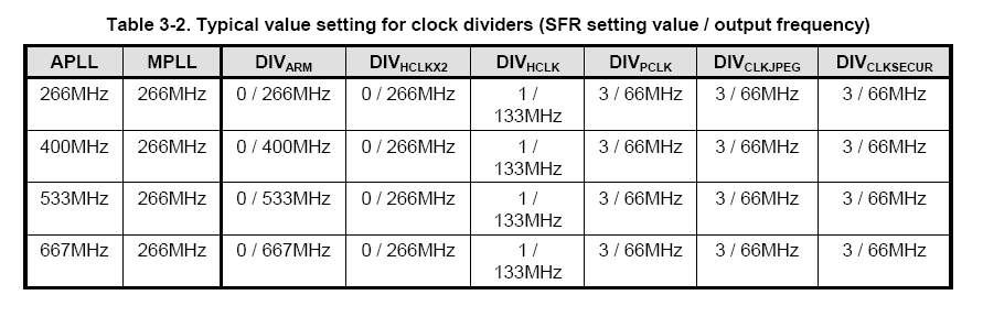
ARM1176最大支持667MHZ,在不改變PLL的情況下,可以通過DIVarm來控制該頻率。
S3C6410由AXI、AHB、APB總線組成。IPs可以連接相應總線來滿足I/O帶寬和操作性能。連接在AXI/AHB的總線上的設備,最高可以達到133MHz的速度。當連接在APB總線上時,最高可以達到66MHz的速度。總線速度很高程度上依賴于AHB和APB總線之間的同步數據傳輸。
ARM and AXI/AHB/APB bus clock generation
ARM1176 processor of S3C6410X runs up to maximum 667MHz. Theoperating frequency can be controlled by the internal clock divider, DIVARM,without changing PLL frequency. The divider ratio varies from 1 to 16. ARM processordecreases the operating speed to reduce power dissipation.S3C6410X consists ofAXI bus, AHB bus, and APB bus to optimize the performance requirements.Internal IPs are connected to appropriate bus systems to meet their I/Obandwidth and operating performance. When they are attached to AXI bus or AHBbus, the operating speed can be up to maximum 133MHz. While they are attachedto APB bus, the maximum operating speed can be up to 66MHz. Moreover, the busspeed between AHB and APB has high dependency to synchronize data transmission.Figure 3-5 illustrates the part of bus clock generation to meet therequirements of bus system clocks.
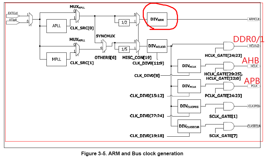
HCLKx2用于兩個DDR控制器,DDR0、DDR1,最高可達到266MHZ,每個DDR控制器可以單獨控制,以用來降低功耗。所有的AHB總線上的時鐘是由DIVhclk分頻得來的,同樣,也可以單獨控制來降低功耗。HCLK_GATE寄存器來配置HCLKx2和HCLK。
APB總線與AHB總線類似,但是注意:在AHB和APB總線之間的頻率比必須隔著一個偶數值,例如:如果DIVhclk是1,那么DIVpclk必須是1、3…..,否則,則不能傳輸數據。
Low-speed interconnection IPs transfer data through APB bus system.APB clocks of them are running at up to 66MHz as described in the above sectionand generated from DIVPCLK clock divider. They are also masked using PCLK_GATEregister. As described, the frequency ratio between AHB clock and APB clockmust be an even integer value. For example, if DIVHCLK has 1 of CLK_DIV0[8],then DIVPCLK must be 1, 3, ... of CLK_DIV0[15:12].Otherwise, the IPs on APB bussystem cannot transfer data correctly.
在AHB總線上的JPEG和安全子系統不能運行在133MHz。AHB總線用DIVjpeg和DIVsecur為它們單獨產生時鐘信號,因此它們與APB之間的頻率也要隔著一個偶數。
APLL單獨用于ARM核,其值不作約束。
其他時鐘,用的時候查看手冊即可。
2)MFC時鐘
3)camera I/F(接口)時鐘
4)顯示時鐘(POST、LCD和scaler
5)音頻時鐘(IIS和PCM)
6)UART、SPI、MMC時鐘
7)IrDA 和USBHOST時鐘
8)時鐘的開關控制
可以通過控制HCLK_GATE、PCLK_GATE、SCLK_GATE。
9)時鐘的輸出
有一個時鐘輸出端口,產生內部時鐘,用于中斷或調試。

評論