ADIADP5034微電源管理(PMU)解決方案

電源管理單元(PMU)評估板主要特性,電路圖,材料清單和元器件布局圖.
本文引用地址:http://www.104case.com/article/178127.htmThe ADP5034 combines two high performance buck regulators and two low dropout (LDO) regulators in a small, 24-lead 4 mm × 4 mm LFCSP to meet demanding performance and board space requirements.
The high switching frequency of the buck regulators enables tiny multilayer external components and minimizes the board space. When the MODE pin is set to high, the buck regulators operate in forced PWM mode. When the MODE pin is set to low, the buck regulators operate in PWM mode when the load is above a pre-defined threshold. When the load current falls below a predefined threshold, the regulator operates in power save mode (PSM), improving the light load efficiency.
The two bucks operate out of phase to reduce the input capacitor requirement. The low quiescent current, low dropout voltage, and wide input voltage range of the ADP5034 LDOs extend the battery life of portable devices. The ADP5034 LDOs maintain power supply rejection greater than 60 dB for frequencies as high as 10 kHz while operating with a low headroom voltage.
Regulators in the ADP5034 are activated through dedicated enable pins. The default output voltages can be externally set in the adjustable version, or factory programmable to a wide range of preset values in the fixed voltage version.
ADP5034主要特性:
Main input voltage range: 2.3 V to 5.5 V
Two 1200 mA buck regulators and two 300 mA LDOs
24-lead, 4 mm × 4 mm LFCSP package
Regulator accuracy: ±3%
Factory programmable or external adjustable VOUTx
3 MHz buck operation with forced PWM and auto PWM/PSM modes
BUCK1/BUCK2: output voltage range from 0.8 V to 3.8 V
LDO1/LDO2: output voltage range from 0.8 V to 5.2 V
LDO1/LDO2: low input supply voltage from 1.7 V to 5.5 V
LDO1/LDO2: high PSRR and low output noise
ADP5034應用:
Power for processors, ASICS, FPGAs, and RF chipsets
Portable instrumentation and medical devices
Space constrained devices
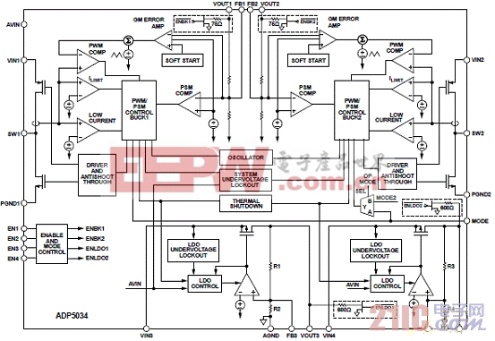
圖1. ADP5034方框圖
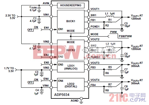
圖2. ADP5034典型應用電路圖
圖3. ADP503采用PSM/PWM控制的處理器系統電源管理圖
圖4. ADP5034帶使能引腳的固定輸出電壓電路圖
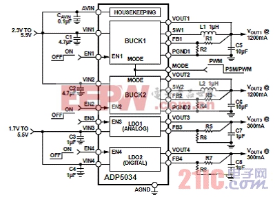
圖5. ADP5034帶使能引腳的可調輸出電壓電路圖
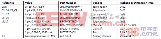
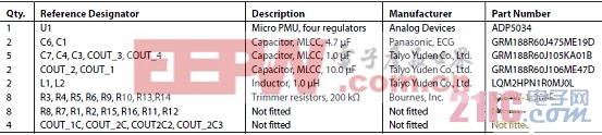
材料清單:
The ADP5034 evaluation board has two step-down regulators with two LDOs that enable evaluation of the ADP5034. The evaluation board is available in standard voltage options.
The ADP5034 uses a proprietary high speed, current mode, constant frequency, pulse-width modulation (PWM) control scheme for excellent stability and transient response. To ensure the longest battery life in portable applications, the ADP5034 features a power save mode (PSM) that reduces the switching frequency under light load conditions, as well as the option to change the mode to fixed PWM operation. The 3 MHz switching frequency minimizes the size of the external components.
The low quiescent current, low dropout voltage, and wide input voltage range of the ADP5034 LDO regulators extend the battery life of portable devices.
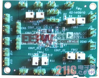
圖6.ADP5034微電源管理單元(PMU)評估板外形圖
ADP5034微電源管理單元(PMU)評估板主要特性:
Full-featured evaluation board for the ADP5034 Standalone capability Simple device measurements, including line and load regulation, demonstrable with A single voltage supply A voltmeter A current meter Load resistors Easy access to external components Cascading options to supply the low dropout (LDO) from either buck Dedicated enable option for each channel Mode option to change bucks from PFM to PWM operation
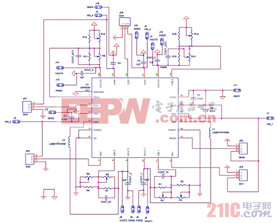
圖7.ADP5034微電源管理單元(PMU)評估板電路圖
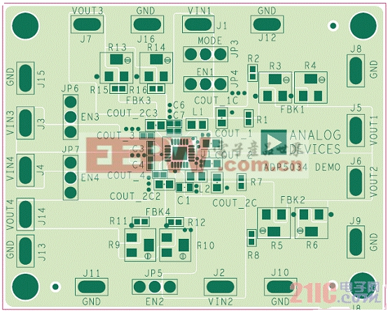
圖8.ADP5034微電源管理單元(PMU)評估板元件布局圖(頂層)
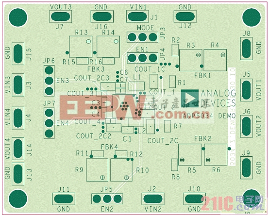
圖9.ADP5034微電源管理單元(PMU)評估板元件布局圖(底層)
ADP5034評估板材料清單:


評論